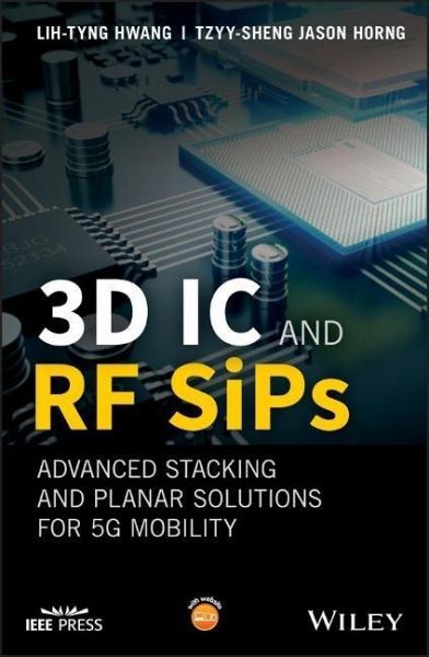
Lih-Tyng Hwang, Tzyy-Sheng Jason Horng
3D IC and RF Sips: Advanced Stacking and Planar Solutions for 5g Mobility
Lih-Tyng Hwang, Tzyy-Sheng Jason Horng
3D IC and RF Sips: Advanced Stacking and Planar Solutions for 5g Mobility
- Gebundenes Buch
- Merkliste
- Auf die Merkliste
- Bewerten Bewerten
- Teilen
- Produkt teilen
- Produkterinnerung
- Produkterinnerung
An interdisciplinary guide to enabling technologies for 3D ICs and 5G mobility, covering packaging, design to product life and reliability assessments _ Features an interdisciplinary approach to the enabling technologies and hardware for 3D ICs and 5G mobility _ Presents statistical treatments and examples with tools that are easily accessible, such as Microsoft's Excel and Minitab _ Fundamental design topics such as electromagnetic design for logic and RF/passives centric circuits are explained in detail _ Provides chapter-wise review questions and powerpoint slides as teaching tools
Andere Kunden interessierten sich auch für
- Ferran MartinBalanced Microwave Filters124,99 €
- Wonbin HongMicrowave and Millimeter-Wave Antenna Design for 5g Smartphone Applications155,99 €
- Anand K. VermaIntroduction to Modern Planar Transmission Lines177,99 €
- He YouRadar Data Processing with Applications191,99 €
- Ferran MartínPlanar Microwave Sensors151,99 €
- Multifunctional Antennas and Arrays for Wireless Communication Systems167,99 €
- Yingjie Jay GuoAdvanced Antenna Array Engineering for 6g and Beyond Wireless Communications156,99 €
-
-
-
An interdisciplinary guide to enabling technologies for 3D ICs and 5G mobility, covering packaging, design to product life and reliability assessments
_ Features an interdisciplinary approach to the enabling technologies and hardware for 3D ICs and 5G mobility
_ Presents statistical treatments and examples with tools that are easily accessible, such as Microsoft's Excel and Minitab
_ Fundamental design topics such as electromagnetic design for logic and RF/passives centric circuits are explained in detail
_ Provides chapter-wise review questions and powerpoint slides as teaching tools
Hinweis: Dieser Artikel kann nur an eine deutsche Lieferadresse ausgeliefert werden.
_ Features an interdisciplinary approach to the enabling technologies and hardware for 3D ICs and 5G mobility
_ Presents statistical treatments and examples with tools that are easily accessible, such as Microsoft's Excel and Minitab
_ Fundamental design topics such as electromagnetic design for logic and RF/passives centric circuits are explained in detail
_ Provides chapter-wise review questions and powerpoint slides as teaching tools
Hinweis: Dieser Artikel kann nur an eine deutsche Lieferadresse ausgeliefert werden.
Produktdetails
- Produktdetails
- Wiley - IEEE
- Verlag: Wiley & Sons / Wiley-IEEE Press
- Artikelnr. des Verlages: 1W119289640
- 1. Auflage
- Seitenzahl: 464
- Erscheinungstermin: 18. Juli 2018
- Englisch
- Abmessung: 239mm x 168mm x 28mm
- Gewicht: 839g
- ISBN-13: 9781119289647
- ISBN-10: 1119289645
- Artikelnr.: 51003462
- Herstellerkennzeichnung
- Libri GmbH
- Europaallee 1
- 36244 Bad Hersfeld
- 06621 890
Lih-Tyng Hwang, National Sun Yat-Sen University, Taiwan, obtained BS degree in Mechanical Engineering from National Tsing-Hua University, Hsinchu, Taiwan, earned PhD degree in Electrical and Systems Engineering from University of Pennsylvania, Philadelphia, Pennsylvania. He started his R&D career with MCNC (Microelectronics Center of North Carolina) in Research Triangle Park, North Carolina. In 1994, he continued his career with SPS (Semiconductor Products Sector), Motorola in Tempe, Arizona. He obtained an MBA degree from ASU while he was with SPS. In 2002, he transferred to Motorola Labs in Schaumburg, Illinois, where he actively worked with Motorola's Mobile division. He began his teaching career with National Sun Yat-Sen University, Kaohsiung, in August, 2009. Jason Tzyy-Sheng Horng, National Sun Yat-Sen University, Taiwan, received the B.S.E.E. degree from National Taiwan University, Taipei, Taiwan, in 1985, and the M.S.E.E. and Ph.D. degrees from the University of California at Los Angeles (UCLA), in 1990 and 1992, respectively. Since August 1992, he has been with the Department of Electrical Engineering, National Sun Yat-Sen University (NSYSU), Kaohsiung, Taiwan, where he was the Director of the Telecommunication Research and Development Center (2003 - 2008) and Director of the Institute of Communications Engineering (2004 - 2007), and where he is currently a Professor. He has authored or coauthored over 100 technical publications published in refereed journals and conferences proceedings. He holds over ten patents. His research interests include RF and microwave integrated circuits and components, RF signal integrity for wireless system-in-package, and digitally assisted RF technologies.
1 MM and MTM for Mobility 1
1.1 Convergence in Communications and the Future, 5G 3
1.1.1 From 1980 (1G) to 2010 (4G) 3
1.1.2 LTE?-A and Rel 10 in 2010s 6
1.1.3 The Future: 5G and IoT (Targeting 2020) 8
1.2 Review of Key Products in Communication Networks 14
1.2.1 Wired Communications 14
1.2.2 Wireless Communications 21
1.3 MM and MTM, an Intro to Hardware Technology 31
1.3.1 Moore's Law 31
1.3.2 More Than Moore 43
1.3.3 MTM Packaging Map and MM? MTM Business Model 53
2 Interconnects 67
2.1 Hierarchy of Interconnection 69
2.1.1 On? Chip (Level 0) Interconnections 69
2.1.2 Peripheral Pads on Semiconductor ICs (Level 0) 72
2.1.3 Al pads (Wirebond and Flip Chip) 73
2.1.4 Cu/Low? K Re?-Distribution Using Damascene Techniques (Flip Chip) 74
2.1.5 Au Pads (III-V) 77
2.1.6 Level 1 Interconnections: WB and FC-Why FC Interconnections are
Preferred? 78
2.2 Level 1, Interconnection Gap in FC?-PBGA, and Level 0.5 80
2.2.1 Wirebonds 80
2.2.2 Flip Chip Bumps with UBM 85
2.2.3 TSV and Microbumps, Cu or Au Stud Bumps (Level 0.5) 91
2.3 Changing Dynamics of Semiconductor Manufacturing 100
2.3.1 Bumping Itself is a Business 100
2.3.2 Cu/Low?-K in BEOL 102
2.3.3 Wafer Fab Foundry and OSAT are Competing for Their Business Shares
102
3 State? of ?the? Art IC Packages, Modules, and Substrates 111
3.1 Single?-Chip Packages (SCPs): Standardized Packages 113
3.1.1 Lead Frame Based: SO, QFP/QFN, and TAB 114
3.1.2 Organic Interposer Based: BGA/CSP and LGA 114
3.1.3 Known Good Bare Die 120
3.1.4 Single?-Chip Packaging Processes 121
3.1.5 IC Testing 123
3.2 Advanced IC Substrates and Assembly 124
3.2.1 MLO Substrates for ICs 126
3.2.2 Multi?-Layered Organic (MLO) for IC Packages 127
3.3 Customized Assemblies: MCP/MCMs and Modules 130
3.3.1 Multi?-Chip Module (MCM) or Multi?-Chip Package (MCP) 131
3.3.2 Modules 132
4 Passives Technology 139
4.1 Thick?-Film Ceramic Technology (TFC) for MLC 146
4.1.1 Green Tapes 146
4.1.2 Thick?-Film Fabrication 149
4.1.3 LTCC EPs, Thick?-Film IPD, and LTCC?-Based RF Modules 151
4.1.4 SMT (or SMD) 155
4.2 MLO Passives by Laminate Organic (LO) 156
4.2.1 MLO?-Based RF Modules 156
4.2.2 Laminates 156
4.2.3 MLO Fabrication 157
4.2.4 MLO EPs and RF Modules 159
4.3 On?-Chip Passives 166
4.3.1 RF Isolation (BCM4330) 166
4.3.2 Monolithic FEOL On?-Chip Passives 168
4.3.3 Rs, Ls, and Cs in BEOL Layers 170
4.3.4 Goals 172
4.4 Thin?-Film Multilayer (TFM) and IPD 173
4.5 Summary on Passives Fabrication Technologies: Solutions for
RF?-Passives Systems 191
5 Electrical Design for 5G Hardware-Digital Focus 199
5.1 Introduction to PCB 201
5.2 Signal Transmission Techniques: Singled?-Ended and Differential Signals
202
5.2.1 Single?-Ended and Differential 202
5.3 Co?-Design Examples 216
5.3.1 Interconnection RF Models and Library 216
5.3.2 Chip?-Package and Chip?-Package?-Board Co?-Designs 219
5.4 Wide I/O Memory Using TSVs 228
5.4.1 JEDEC Memory Standards 230
5.4.2 Data Structure Using TSV?-Based Wide I/O 230
6 Electrical Design for 5G Hardware-RF Focus 239
6.1 PHY, Modulated RF Carriers; a PoP Possible? 240
6.1.1 Frequency Bands and Wave Propagation Characteristics 240
6.1.2 Narrow?-Band Process and CW Carrier for Digital Signals 242
6.2 Antennas 244
6.2.1 Two Often Encountered RF Passive Structures in Modern Portable
Electronics: Antenna and Its Feed 244
6.2.2 Types of Antennas: Linear, Microstrip?-Patch, and Multi?-Element
Antenna 245
6.2.3 Active?-Integrated Antennas and Measurement of Antenna Performance
251
6.3 RF Functional Components 256
6.3.1 Bandpass Filters 256
6.3.2 Baluns 257
6.3.3 Switches and Duplexers 262
6.4 EMI/EMC 263
6.4.1 Sources of Interference 264
6.4.2 Diagnostic and Regulations Conformation Techniques 264
6.4.3 Containment Techniques 267
7 Product, Process Development, and Control 271
7.1 Business Processes 272
7.1.1 Strategic Management (Product and Process Development) 272
7.1.2 Design and Manufacturing; Outsourced or Not 273
7.2 History of Statistical Approach for Quality Management 273
7.2.1 Quality Guidelines and Standards 274
7.2.2 Semiconductor Process Development and Characterization 274
7.3 APQP-An Iterative Process for Product and Process Development 275
7.3.1 Translate Product Ideas Into Processes 275
7.4 FMEA, Control Plan, and Initial Process Study 276
7.4.1 RPN 276
7.4.2 Locating the Root Causes 281
7.4.3 Pre?-Launch Control Plan 283
7.4.4 Initial Process Study 284
7.5 PPAP and SPC 287
7.5.1 PPAP 287
7.5.2 SPC 287
8 Product Life and Reliability Assessment 291
8.1 Product Life Prediction 292
8.1.1 Calculate MTTF from Processes and Theoretical Distributions 293
8.1.2 Practices to Obtain the Expected Product Life 296
8.1.3 Activation Energy 300
8.2 Reliability Assessment 301
8.2.1 Assessment Variables for Reliability Tests 302
8.2.2 Reliability Assessment Practices 303
8.2.3 Discussions on Weibull Analysis and Weibull Plotting 309
9 Hardware Solutions for 5G Mobility 317
9.1 5G Mobility Products and Planar Solutions 318
9.1.1 High?-Density and Logic Products 319
9.1.2 RF?-Passives Systems 326
9.1.3 A Summary: WLP and LPP Used for Both HD&L and RF?-Passives Products
333
9.2 Advanced Interconnection and Future Business Model 336
9.2.1 Advanced Interconnection 336
9.2.2 New Business Model 341
9.3 Finale-What's Not 343
9.3.1 New from Wafer Foundries 343
9.3.2 System and Architectural Design of Mobile Handsets 345
9.3.3 Thermo?-Mechanical and Thermal Science 349
9.3.4 Sensors and IoT 349
A Failure Mechanisms and Failure Analysis 357
A.1 Failure Mechanisms, or Macroscopic Models 358
A.1.1 Silicon Oxide Breakdown 359
A.1.2 Stress?-Induced Migration (SM) 360
A.1.3 Electro?-Migration (EM) and Hillocks 360
A.1.4 Spiking 362
A.1.5 IMC, Purple plague (Gold?-Al Intermetallics) 363
A.1.6 Fatigue and Creeping 364
A.1.7 Die Cracking 366
A.1.8 Delamination and Popcorning 366
A.1.9 Corrosion 367
A.2 Failure Analysis (FA) Techniques and FA Tools 368
A.2.1 De?-Processing (or De?-Capping) Techniques 368
A.2.2 Microscopic and Analytical Tools 369
B ANOVA 375
B.1 One?-Way ANOVA 376
B.2 Two?-Way ANOVA 377
C Gauge R&R and DOE 381
C.1 GR&R 381
C.1.1 AIAG's Xbar/Range Method for Gauge R&R Study 381
C.1.2 Minitab 383
C.1.3 GR&R Casted in the ANOVA Format 383
C.1.4 Criteria 384
C.2 DOE 384
C.2.1 DOE Guidelines 385
C.2.2 2k Runs, Unreplicated Case 386
C.2.3 Fractional Factorial Designs, 2k?-p Run, p = 1, 2,.., < k 399
D Statistics Tables 409
D.1 F Distribution 409 D.2 Poisson Table of Expected # of Occurrences at a
Confidence Level (C.L.) 409
D.3 MR Percentile Table 409