37,99 €
inkl. MwSt.
Versandkostenfrei*
Versandfertig in 6-10 Tagen
payback
19 °P sammeln
  • Gebundenes Buch

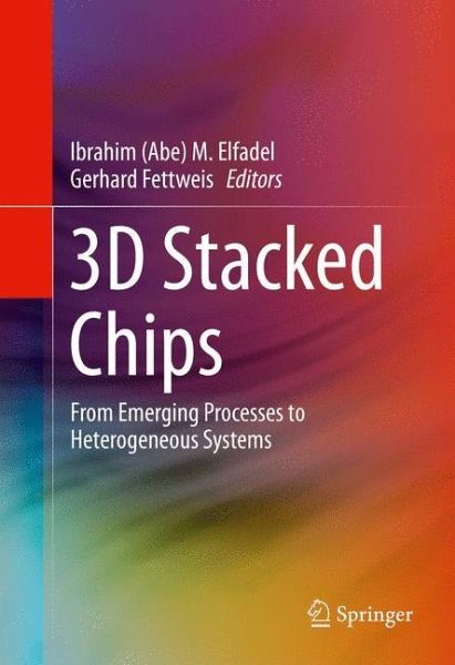
This book explains for readers how 3D chip stacks promise to increase the level of on-chip integration, and to design new heterogeneous semiconductor devices that combine chips of different integration technologies (incl. sensors) in a single package of the smallest possible size. The authors focus on heterogeneous 3D integration, addressing some of the most important challenges in this emerging technology, including contactless, optics-based, and carbon-nanotube-based 3D integration, as well as signal-integrity and thermal management issues in copper-based 3D integration. Coverage also…mehr

Produktbeschreibung
This book explains for readers how 3D chip stacks promise to increase the level of on-chip integration, and to design new heterogeneous semiconductor devices that combine chips of different integration technologies (incl. sensors) in a single package of the smallest possible size. The authors focus on heterogeneous 3D integration, addressing some of the most important challenges in this emerging technology, including contactless, optics-based, and carbon-nanotube-based 3D integration, as well as signal-integrity and thermal management issues in copper-based 3D integration. Coverage also includes the 3D heterogeneous integration of power sources, photonic devices, and non-volatile memories based on new materials systems.
Autorenporträt
 Ibrahim (Abe) M. Elfadel has 15 years of industrial experience in the research, development and deployment of advanced computer-aided design (CAD) tools and methodologies for deep-submicron, high-performance digital designs. Most recently, he played a key role in the development and deployment of IBM's next-generation layout verification tools for the ultra-deep submicron CMOS technology nodes. Dr. Elfadel is the recipient of six Invention Achievement Awards, an Outstanding Technical Achievement Award and a Research Division Award, all from IBM, for his contributions in the area of VLSI CAD.  He is currently serving as an Associate Editor for the IEEE Transactions on Computer-Aided Design for Integrated Circuits and Systems. Gerhard Fettweis earned his Ph.D. under H. Meyr's supervision from RWTH Aachen in 1990. After one year at IBM Research in San Jose, CA he moved to TCSI Inc., Berkeley, CA. Since 1994 he is Vodafone Chair Professor at TU Dresden, Germany, with currently 20 companies from Asia/Europe/US sponsoring his research on wireless transmission and chip design. He coordinates 2 DFG centers at TU Dresden, cfAED and HAEC. Gerhard is IEEE Fellow, member of acatech, has an honorary doctorate from TU Tampere, and has received multiple awards. In Dresden he has spun-out ten start-ups, and setup funded projects of more than EUR 1/3 billion volume. He has helped organized IEEE conferences, most notably as TPC Chair of IEEE ICC 2009, IEEE TTM 2012, and Ge neral Chair of VTC Spring 2013. He remains active within IEEE.  
Rezensionen
"The book is valuable as a learning tool for 3D stacked chips through TSVs ... . a valuable addition to a scientific library, as well as served as good introduction for device reliability engineers or specialists and industrials involved in the field of 3D stacking in wafer fabrication and integrated circuit design. ... highly recommended for people who desire a better understanding of the theory and practice of 3D TSVs and technical considerations in 3D chips floorplanning, modeling and characterization." (Chong Leong Gan and Uda Hashim, Microelectronics Reliability, Vol. 63, August, 2016)