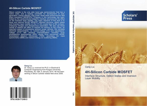
4H-Silicon Carbide MOSFET
Interface Structure, Defect States and Inversion Layer Mobility
Versandkostenfrei!
Versandfertig in 6-10 Tagen
40,99 €
inkl. MwSt.

PAYBACK Punkte
20 °P sammeln!
Silicon carbide is the only wide band gap semiconductor that has a native oxide, and a leading candidate for development of next-generation, energy efficient, high power metal-oxide-semiconductor field effect transistors (MOSFETs). Progress in this technology has been limited by the semiconductor-dielectric interface structure and its effect on the inversion layer mobility. The major objective of this work is to study and improve 4H-SiC MOSFET interface structure, defect states and inversion layer mobility on the (11-20) crystal face of SiC (a-face), employing nitrogen and phosphorous passivat...
Silicon carbide is the only wide band gap semiconductor that has a native oxide, and a leading candidate for development of next-generation, energy efficient, high power metal-oxide-semiconductor field effect transistors (MOSFETs). Progress in this technology has been limited by the semiconductor-dielectric interface structure and its effect on the inversion layer mobility. The major objective of this work is to study and improve 4H-SiC MOSFET interface structure, defect states and inversion layer mobility on the (11-20) crystal face of SiC (a-face), employing nitrogen and phosphorous passivation. We also use these results to explore the effect of reactive ion etching on the a-face, an important aspect of processing optimum power devices. We correlate electrical measurements, i.e. current-voltage (I-V) and capacitance-voltage (C-V) with physical characterization including X-ray photoelectron spectroscopy (XPS), atomic force microscopy (AFM), transmission electron microscopy (TEM), secondary ion mass spectrometry (SIMS) and medium energy ion scattering (MEIS).


