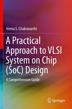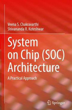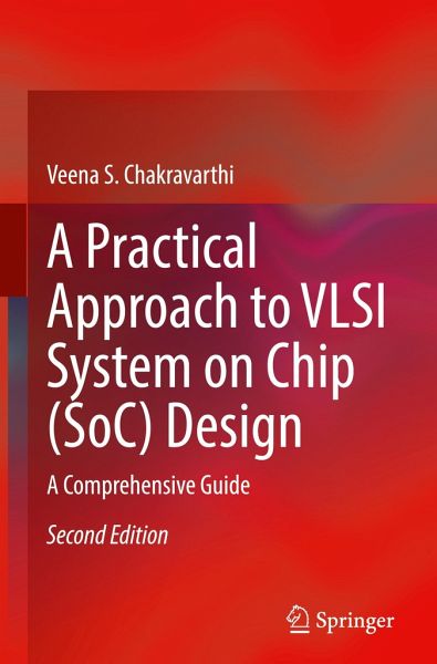
A Practical Approach to VLSI System on Chip (SoC) Design
A Comprehensive Guide
Versandkostenfrei!
Versandfertig in 6-10 Tagen
91,99 €
inkl. MwSt.
Weitere Ausgaben:

PAYBACK Punkte
46 °P sammeln!
Now in a thoroughly revised second edition, this practical practitioner guide provides a comprehensive overview of the SoC design process. It explains end-to-end system on chip (SoC) design processes and includes updated coverage of design methodology, the design environment, EDA tool flow, design decisions, choice of design intellectual property (IP) cores, sign-off procedures, and design infrastructure requirements. The second edition provides new information on SOC trends and updated design cases. Coverage also includes critical advanced guidance on the latest UPF-based low power design flo...
Now in a thoroughly revised second edition, this practical practitioner guide provides a comprehensive overview of the SoC design process. It explains end-to-end system on chip (SoC) design processes and includes updated coverage of design methodology, the design environment, EDA tool flow, design decisions, choice of design intellectual property (IP) cores, sign-off procedures, and design infrastructure requirements. The second edition provides new information on SOC trends and updated design cases. Coverage also includes critical advanced guidance on the latest UPF-based low power design flow, challenges of deep submicron technologies, and 3D design fundamentals, which will prepare the readers for the challenges of working at the nanotechnology scale.
A Practical Approach to VLSI System on Chip (SoC) Design: A Comprehensive Guide, Second Edition provides engineers who aspire to become VLSI designers with all the necessary information and details of EDA tools. It willbe a valuable professional reference for those working on VLSI design and verification portfolios in complex SoC designs
A Practical Approach to VLSI System on Chip (SoC) Design: A Comprehensive Guide, Second Edition provides engineers who aspire to become VLSI designers with all the necessary information and details of EDA tools. It willbe a valuable professional reference for those working on VLSI design and verification portfolios in complex SoC designs


