Aberration-Corrected Analytical Transmission Electron Microscopy
Herausgegeben von Brydson, Rik
Aberration-Corrected Analytical Transmission Electron Microscopy
Herausgegeben von Brydson, Rik
- Gebundenes Buch
- Merkliste
- Auf die Merkliste
- Bewerten Bewerten
- Teilen
- Produkt teilen
- Produkterinnerung
- Produkterinnerung
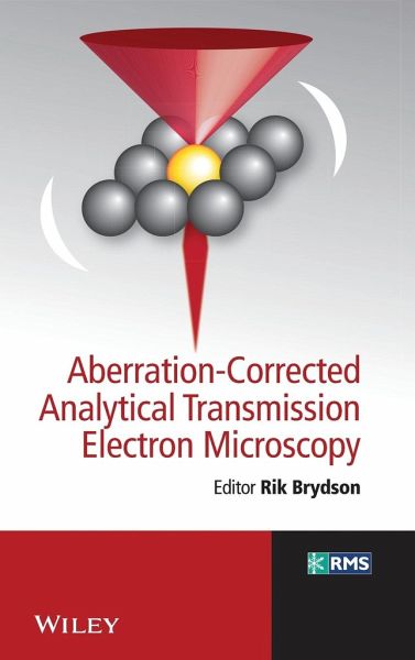
The book is concerned with the theory, background, and practical use of transmission electron microscopes with lens correctors that can correct the effects of spherical aberration. The book also covers a comparison with aberration correction in the TEM and applications of analytical aberration corrected STEM in materials science and biology. This book is essential for microscopists involved in nanoscale and materials microanalysis especially those using scanning transmission electron microscopy, and related analytical techniques such as electron diffraction x-ray spectrometry (EDXS) and electron energy loss spectroscopy (EELS).…mehr
Andere Kunden interessierten sich auch für
- Günther WyszeckiColor Science159,99 €
- Arne ValbergLight Vision Color102,99 €
- Shin-Tson WuAdaptive Lenses146,99 €
- Lihong V. WangBiomedical Optics172,99 €
- John A. BuckFundamentals of Optical Fibers179,99 €
- Bernard C. KressDigital Diffractive Optics441,99 €
- F Graham SmithOptics and Photonics277,99 €
-
-
-
The book is concerned with the theory, background, and practical use of transmission electron microscopes with lens correctors that can correct the effects of spherical aberration. The book also covers a comparison with aberration correction in the TEM and applications of analytical aberration corrected STEM in materials science and biology. This book is essential for microscopists involved in nanoscale and materials microanalysis especially those using scanning transmission electron microscopy, and related analytical techniques such as electron diffraction x-ray spectrometry (EDXS) and electron energy loss spectroscopy (EELS).
Hinweis: Dieser Artikel kann nur an eine deutsche Lieferadresse ausgeliefert werden.
Produktdetails
- Produktdetails
- RMS - Royal Microscopical Society
- Verlag: Wiley & Sons
- 1. Auflage
- Seitenzahl: 304
- Erscheinungstermin: 26. September 2011
- Englisch
- Abmessung: 235mm x 157mm x 21mm
- Gewicht: 598g
- ISBN-13: 9780470518519
- ISBN-10: 0470518510
- Artikelnr.: 33368169
- Herstellerkennzeichnung
- Libri GmbH
- Europaallee 1
- 36244 Bad Hersfeld
- 06621 890
Professor R.M.D. (Rik) Brydson is based in the School of Process, Environmental and Materials Engineering at the University of Leeds, UK. He is a committee member for the European Microscopy Society as well as the Electron Microscopy and Analysis Group (Institute of Physics).
List of Contributors xi Preface xiii 1 General Introduction to Transmission Electron Microscopy (TEM) 1 Peter Goodhew 1.1 What TEM Offers 1 1.2 Electron Scattering 3 1.2.1 Elastic Scattering 7 1.2.2 Inelastic Scattering 8 1.3 Signals which could be Collected 10 1.4 Image Computing 12 1.4.1 Image Processing 12 1.4.2 Image Simulation 13 1.5 Requirements of a Specimen 14 1.6 STEM Versus CTEM 17 1.7 Two Dimensional and Three Dimensional Information 17 2 Introduction to Electron Optics 21 Gordon Tatlock 2.1 Revision of Microscopy with Visible Light and Electrons 21 2.2 Fresnel and Fraunhofer Diffraction 22 2.3 Image Resolution 23 2.4 Electron Lenses 25 2.4.1 Electron Trajectories 26 2.4.2 Aberrations 27 2.5 Electron Sources 30 2.6 Probe Forming Optics and Apertures 32 2.7 SEM, TEM and STEM 33 3 Development of STEM 39 L.M. Brown 3.1 Introduction: Structural and Analytical Information in Electron Microscopy 39 3.2 The Crewe Revolution: How STEM Solves the Information Problem 41 3.3 Electron Optical Simplicity of STEM 42 3.4 The Signal Freedom of STEM 45 3.4.1 Bright-Field Detector (Phase Contrast, Diffraction Contrast) 45 3.4.2 ADF, HAADF 45 3.4.3 Nanodiffraction 46 3.4.4 EELS 47 3.4.5 EDX 47 3.4.6 Other Techniques 48 3.5 Beam Damage and Beam Writing 48 3.6 Correction of Spherical Aberration 49 3.7 What does the Future Hold? 51 4 Lens Aberrations: Diagnosis and Correction 55 Andrew Bleloch and Quentin Ramasse 4.1 Introduction 55 4.2 Geometric Lens Aberrations and Their Classification 59 4.3 Spherical Aberration-Correctors 66 4.3.1 Quadrupole-Octupole Corrector 69 4.3.2 Hexapole Corrector 70 4.3.3 Parasitic Aberrations 72 4.4 Getting Around Chromatic Aberrations 74 4.5 Diagnosing Lens Aberrations 75 4.5.1 Image-based Methods 77 4.5.2 Ronchigram-based Methods 80 4.5.3 Precision Needed 85 4.6 Fifth Order Aberration-Correction 85 4.7 Conclusions 86 5 Theory and Simulations of STEM Imaging 89 Peter D. Nellist 5.1 Introduction 89 5.2 Z-Contrast Imaging of Single Atoms 90 5.3 STEM Imaging Of Crystalline Materials 92 5.3.1 Bright-field Imaging and Phase Contrast 93 5.3.2 Annular Dark-field Imaging 96 5.4 Incoherent Imaging with Dynamical Scattering 101 5.5 Thermal Diffuse Scattering 103 5.5.1 Approximations for Phonon Scattering 104 5.6 Methods of Simulation for ADF Imaging 106 5.6.1 Absorptive Potentials 106 5.6.2 Frozen Phonon Approach 107 5.7 Conclusions 108 6 Details of STEM 111 Alan Craven 6.1 Signal to Noise Ratio and Some of its Implications 112 6.2 The Relationships Between Probe Size, Probe Current and Probe Angle 113 6.2.1 The Geometric Model Revisited 113 6.2.2 The Minimum Probe Size, the Optimum Angle and the Probe Current 115 6.2.3 The Probe Current 115 6.2.4 A Simple Approximation to Wave Optical Probe Size 117 6.2.5 The Effect of Chromatic Aberration 117 6.2.6 Choosing
opt in Practice 118 6.2.7 The Effect of Making a Small Error in the Choice of
opt 119 6.2.8 The Effect of
On the Diffraction Pattern 120 6.2.9 Probe Spreading and Depth of Field 122 6.3 The Condenser System 124 6.4 The Scanning System 126 6.4.1 Principles of the Scanning System 126 6.4.2 Implementation of the Scanning System 128 6.4.3 Deviations of the Scanning System From Ideality 128 6.4.4 The Relationship Between Pixel Size and Probe Size 130 6.4.5 Drift, Drift Correction and Smart Acquisition 131 6.5 The Specimen Stage 133 6.6 Post-Specimen Optics 135 6.7 Beam Blanking 136 6.8 Detectors 137 6.8.1 Basic Properties of a Detector 137 6.8.2 Single and Array Detectors 139 6.8.3 Scintillator/Photomultiplier Detector 139 6.8.4 Semiconductor Detectors 141 6.8.5 CCD Cameras 142 6.9 Imaging Using Transmitted Electrons 145 6.9.1 The Diffraction Pattern 145 6.9.2 Coherent Effects in the Diffraction Pattern 147 6.9.3 Small Angular Range - Bright Field and Tilted Dark Field Images 152 6.9.4 Medium Angular Range - MAADF 152 6.9.5 High Angular Range - HAADF 153 6.9.6 Configured Detectors 153 6.10 Signal Acquisition 154 Acknowledgements 159 7 Electron Energy Loss Spectrometry and Energy Dispersive X-ray Analysis 163 Rik Brydson and Nicole Hondow 7.1 What is EELS and EDX? 164 7.1.1 Basics of EDX 164 7.1.2 Basics of EELS 166 7.1.3 Common Features For Analytical Spectrometries 168 7.2 Analytical Spectrometries in the Environment of the Electron Microscope 170 7.2.1 Instrumentation for EDX 170 7.2.2 EELS Instrumentation 174 7.2.3 Microscope Instrumentation for Analytical Spectroscopies 178 7.3 Elemental Analysis and Quantification Using EDX 182 7.4 Low Loss EELS - Plasmons, IB Transitions and Band Gaps 187 7.5 Core Loss EELS 191 7.5.1 Elemental Quantification 191 7.5.2 Near-Edge Fine Structure For Chemical and Bonding Analysis 195 7.5.3 Extended-Edge Fine Structure For Bonding Analysis 200 7.6 EDX and EELS Spectral Modelling 201 7.6.1 Total Spectrum Modelling 201 7.6.2 EELS Modelling of Near Edge Structures and also the Low Loss 201 7.7 Spectrum Imaging: EDX and EELS 202 7.8 Ultimate Spatial Resolution of EELS 206 7.9 Conclusion 207 8 Applications of Aberration-Corrected Scanning Transmission Electron Microscopy 211 Mervyn D. Shannon 8.1 Introduction 211 8.2 Sample Condition 212 8.3 HAADF Imaging 213 8.3.1 Imaging of Isolated Atoms 213 8.3.2 Line Defects (1-D) 219 8.3.3 Interfaces and Extended Defects (2-D) 220 8.3.4 Detailed Particle Structures (3-D) 226 8.3.5 Low-loss EELS 230 8.3.6 Core-loss EELS and Atomic-scale Spectroscopic Imaging 231 8.4 Conclusions 236 9 Aberration-Corrected Imaging in CTEM 241 Sarah J. Haigh and Angus I. Kirkland 9.1 Introduction 241 9.2 Optics and Instrumentation for Aberration-Corrected CTEM 243 9.2.1 Aberration-Correctors 243 9.2.2 Related Instrumental Developments 243 9.3 CTEM Imaging Theory 244 9.3.1 CTEM Image Formation 244 9.3.2 The Wave Aberration Function 246 9.3.3 Partial Coherence 252 9.4 Corrected Imaging Conditions 253 9.4.1 The Use of Negative Spherical Aberration 254 9.4.2 Amplitude Contrast Imaging 256 9.5 Aberration Measurement 256 9.5.1 Aberration Measurement From Image Shifts 256 9.5.2 Aberration Measurement from Diffractograms 257 9.5.3 An Alternative Approach to Aberration Measurement 258 9.6 Indirect Aberration Compensation 258 9.7 Advantages of Aberration-Correction for CTEM 259 9.8 Conclusions 259 Acknowledgements 260 Appendix A: Aberration Notation 263 Appendix B: General Notation 267 Index 275