Mikhail Baklanov, Paul S. Ho, Ehrenfried Zschech
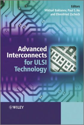
Advanced Interconnects for ULSI Technology
Herausgeber: Baklanov, Mikhail; Zschech, Ehrenfried; Ho, Paul S
Mikhail Baklanov, Paul S. Ho, Ehrenfried Zschech
Advanced Interconnects for ULSI Technology
Herausgeber: Baklanov, Mikhail; Zschech, Ehrenfried; Ho, Paul S
- Gebundenes Buch
- Merkliste
- Auf die Merkliste
- Bewerten Bewerten
- Teilen
- Produkt teilen
- Produkterinnerung
- Produkterinnerung
Finding new materials for copper/low-k interconnects is critical to the continuing development of computer chips. While copper/low-k interconnects have served well, allowing for the creation of Ultra Large Scale Integration (ULSI) devices which combine over a billion transistors onto a single chip, the increased resistance and RC-delay at the smaller scale has become a significant factor affecting chip performance.
Advanced Interconnects for ULSI Technology is dedicated to the materials and methods which might be suitable replacements. It covers a broad range of topics, from physical…mehr
Andere Kunden interessierten sich auch für
- Tak-Kei LamBoolean Circuit Rewiring167,99 €
- KitaiPrinciples of Solar Cells, LEDs219,99 €
- Handbook of 3D Integration155,99 €
- Eishi H. IbeTerrestrial Radiation Effects in ULSI Devices and Electronic Systems174,99 €
- Yasuhisa OmuraSoi Lubistors191,99 €
- Yaguang LianSemiconductor Microchips and Fabrication140,99 €
- Chris MackFundamental Principles of Optical77,99 €
-
-
-
Finding new materials for copper/low-k interconnects is critical to the continuing development of computer chips. While copper/low-k interconnects have served well, allowing for the creation of Ultra Large Scale Integration (ULSI) devices which combine over a billion transistors onto a single chip, the increased resistance and RC-delay at the smaller scale has become a significant factor affecting chip performance.
Advanced Interconnects for ULSI Technology is dedicated to the materials and methods which might be suitable replacements. It covers a broad range of topics, from physical principles to design, fabrication, characterization, and application of new materials for nano-interconnects, and discusses:
Interconnect functions, characterisations, electrical properties and wiring requirements
Low-k materials: fundamentals, advances and mechanical properties
Conductive layers and barriers
Integration and reliability including mechanical reliability, electromigration and electrical breakdown
New approaches including 3D, optical, wireless interchip, and carbon-based interconnects
Intended for postgraduate students and researchers, in academia and industry, this book provides a critical overview of the enabling technology at the heart of the future development of computer chips.
Hinweis: Dieser Artikel kann nur an eine deutsche Lieferadresse ausgeliefert werden.
Advanced Interconnects for ULSI Technology is dedicated to the materials and methods which might be suitable replacements. It covers a broad range of topics, from physical principles to design, fabrication, characterization, and application of new materials for nano-interconnects, and discusses:
Interconnect functions, characterisations, electrical properties and wiring requirements
Low-k materials: fundamentals, advances and mechanical properties
Conductive layers and barriers
Integration and reliability including mechanical reliability, electromigration and electrical breakdown
New approaches including 3D, optical, wireless interchip, and carbon-based interconnects
Intended for postgraduate students and researchers, in academia and industry, this book provides a critical overview of the enabling technology at the heart of the future development of computer chips.
Hinweis: Dieser Artikel kann nur an eine deutsche Lieferadresse ausgeliefert werden.
Produktdetails
- Produktdetails
- Verlag: Wiley & Sons
- 1. Auflage
- Seitenzahl: 608
- Erscheinungstermin: 2. April 2012
- Englisch
- Abmessung: 261mm x 177mm x 33mm
- Gewicht: 1069g
- ISBN-13: 9780470662540
- ISBN-10: 0470662549
- Artikelnr.: 34412474
- Herstellerkennzeichnung
- Libri GmbH
- Europaallee 1
- 36244 Bad Hersfeld
- 06621 890
Mikhail R. Baklanov IMEC, Leuven, Belgium Paul S. Ho Laboratory for Interconnect and Packaging, University of Texas at Austin, Austin, Texas, USA Ehrenfried Zschech Fraunhofer Institute for Nondestructive Testing, Dresden, Germany
About the Editors xv
List of Contributors xvii
Preface xxi
List of Abbreviations xxv
Section I Low-k Materials 1
1 Low-k Materials: Recent Advances 3
Geraud Dubois and Willi Volksen
1.1 Introduction 3
1.2 Integration Challenges 5
1.2.1 Process-Induced Damage 6
1.2.2 Mechanical Properties 9
1.3 Processing Approaches to Existing Integration Issues 10
1.3.1 Post-deposition Treatments 11
1.3.2 Prevention or Repair of Plasma-Induced Processing Damage 14
1.3.3 Multilayer Structures 15
1.4 Material Advances to Overcome Current Limitations 16
1.4.1 Silica Zeolites 16
1.4.2 Hybrid Organic-Inorganic: Oxycarbosilanes 19
1.5 Conclusion 22
2 Ultra-Low-k by CVD: Deposition and Curing 35
Vincent Jousseaume, Aziz Zenasni, Olivier Gourhant, Laurent Favennec and
Mikhail R. Baklanov
2.1 Introduction 35
2.2 Porogen Approach by PECVD 37
2.2.1 Precursors and Deposition Conditions 37
2.2.2 Mystery Still Unsolved: From Porogens to Pores 41
2.3 UV Curing 42
2.3.1 General Overview of Curing 42
2.3.2 UV Curing Mechanisms 43
2.4 Impact of Curing on Structure and Physical Properties: Benefits of UV
Curing 49
2.4.1 Porosity 49
2.4.2 Chemical Structure and Mechanical Properties 50
2.4.3 Electrical Properties 56
2.5 Limit/Issues with the Porogen Approach 57
2.5.1 Porosity Creation Limit 58
2.5.2 Porogen Residues 59
2.6 Future of CVD Low-k 62
2.6.1 New Matrix Precursor 62
2.6.2 Other Deposition Strategies 64
2.6.3 New Deposition Techniques 66
2.7 Material Engineering: Adaptation to Integration Schemes 68
2.8 Conclusion 70
3 Plasma Processing of Low-k Dielectrics 79
Hualing Shi, Denis Shamiryan, Jean-Francois de Marneffe, Huai Huang, Paul
S. Ho and Mikhail R. Baklanov
3.1 Introduction 79
3.2 Materials and Equipment 80
3.3 Process Results Characterization 82
3.4 Interaction of Low-k Dielectrics with Plasma 85
3.4.1 Low-k Etch Chemistries 85
3.4.2 Patterning Strategies and Masking Materials 87
3.4.3 Etch Mechanisms 88
3.5 Mechanisms of Plasma Damage 92
3.5.1 Gap Structure Studies 93
3.5.2 Effect of Radical Density 95
3.5.3 Effect of Ion Energy 96
3.5.4 Effect of Photon Energy and Intensity 99
3.5.5 Plasma Damage by Oxidative Radicals 103
3.5.6 Hydrogen-Based Plasma 105
3.5.7 Minimization of Plasma Damage 108
3.6 Dielectric Recovery 112
3.6.1 CH4 Beam Treatment 112
3.6.2 Dielectric Recovery by Silylation 113
3.6.3 UV Radiation 119
3.7 Conclusions 121
4 Wet Clean Applications in Porous Low-k Patterning Processes 129
Quoc Toan Le, Guy Vereecke, Herbert Struyf, Els Kesters and Mikhail R.
Baklanov
4.1 Introduction 129
4.2 Silica and Porous Hybrid Dielectric Materials 130
4.3 Impact of Plasma and Subsequent Wet Clean Processes on the Stability of
Porous Low-k Dielectrics 134
4.3.1 Stability in Pure Chemical Solutions 134
4.3.2 Stability in Commercial Chemistries 135
4.3.3 Hydrophobicity of Hybrid Low-k Materials 138
4.4 Removal of Post-Etch Residues and Copper Surface Cleaning 141
4.5 Plasma Modification and Removal of Post-Etch 193 nm Photoresist 146
4.5.1 Modification of 193 nm Photoresist by Plasma Etch 146
4.5.2 Wet Removal of 193 nm Photoresist 153
Section II Conductive Layers and Barriers 173
5 Copper Electroplating for On-Chip Metallization 175
Valery M. Dubin
5.1 Introduction 175
5.2 Copper Electroplating Techniques 176
5.3 Copper Electroplating Superfill 177
5.3.1 The Role of Accelerator 177
5.3.2 The Role of Suppressor 178
5.3.3 The Role of Leveler 180
5.4 Alternative Cu Plating Methods 182
5.4.1 Electroless Plating 182
5.4.2 Direct Plating 182
5.5 Electroplated Cu Properties 184
5.5.1 Resistivity 184
5.5.2 Impurities 184
5.5.3 Electromigration 185
5.6 Conclusions 186
6 Diffusion Barriers 193
Michael Hecker and René Hübner
6.1 Introduction 193
6.1.1 Cu Metallization, Barrier Requirements and Materials 193
6.1.2 Barrier Deposition Techniques 195
6.1.3 Characterization of Barrier Performance 196
6.2 Metal-Based Barriers as Liners for Cu Seed Deposition 198
6.2.1 Ta-Based Barriers 198
6.2.2 W-Based Barriers 209
6.2.3 Ti-Based Barriers 210
6.2.4 Further Systems 211
6.3 Advanced Barrier Approaches 212
6.3.1 Barriers for Direct Cu Plating 212
6.3.2 Metal Capping Layers 214
6.3.3 Self-Forming Diffusion Barriers 216
6.3.4 Self-Assembled Molecular Nanolayers and Polymer-Based Barriers 218
6.4 Conclusions 221
Section III Integration and Reliability 235
7 Integration and Electrical Properties 237
Sridhar Balakrishnan, Ruth Brain and Larry Zhao
7.1 Introduction 237
7.2 On-Die Interconnects in the Submicrometer Era 237
7.3 On-Die Interconnects at Sub-100 nm Nodes 240
7.4 Integration of Low-k Dielectrics in Sub-65 nm Nodes 241
7.4.1 Degradation of Dielectric Constant during Integration 243
7.4.2 Integration Issues in ELK Dielectrics Due to Degraded Mechanical
Properties 246
7.5 Patterning Integration at Sub-65 nm Nodes 248
7.5.1 Patterning Challenges 249
7.6 Integration of Conductors in Sub-65 nm Nodes 252
7.6.1 Narrow Line Copper Resistivity 253
7.6.2 Integrating Novel Barrier/Liner Materials and Deposition Techniques
for Cu Interconnects 254
7.6.3 Self-Forming Barriers and Their Integration 256
7.6.4 Integration to Enable Reliable Copper Interconnects 257
7.7 Novel Air-Gap Interconnects 258
7.7.1 Unlanded Via Integration with Air-Gap Interconnects 258
7.7.2 Air-Gap Formation Using Nonconformal Dielectric Deposition 259
7.7.3 Air-Gap Formation Using a Sacrificial Material 260
8 Chemical Mechanical Planarization for Cu-Low-k Integration 267
Gautam Banerjee
8.1 Introduction 267
8.2 Back to Basics 268
8.3 Mechanism of the CMP Process 268
8.4 CMP Consumables 271
8.4.1 Slurry 271
8.4.2 Pad 273
8.4.3 Pad Conditioner 274
8.5 CMP Interactions 276
8.6 Post-CMP Cleaning 281
8.6.1 Other Defects 286
8.6.2 Surface Finish 286
8.6.3 E-Test 287
8.7 Future Direction 287
References 288
9 Scaling and Microstructure Effects on Electromigration Reliability for Cu
Interconnects 291
Chao-Kun Hu, René Hübner, Lijuan Zhang, Meike Hauschildt and Paul S. Ho
9.1 Introduction 291
9.2 Electromigration Fundamentals 293
9.2.1 EM Mass Flow 293
9.2.2 EM Lifetime and Scaling Rule 294
9.2.3 Statistical Test Method 296
9.2.4 Effect of Current Density on EM Lifetime 298
9.3 Cu Microstructure 300
9.3.1 X-ray Diffraction (XRD) 300
9.3.2 Electron Backscatter Diffraction in the Scanning Electron Microscope
302
9.3.3 Orientation Imaging Microscopy in the Transmission Electron
Microscope 304
9.4 Lifetime Enhancement 306
9.4.1 Effect of a Ta Liner 306
9.4.2 Upper-Level Dummy Vias 308
9.4.3 Plasma Pre-clean and SiH4 Soak 310
9.4.4 CVD and ECD Cu and the Effect of Nonmetallic Impurities 311
9.4.5 Cu Alloys 314
9.4.6 CoWP Cap Near-Bamboo and Polycrystalline Cu Lines 319
9.5 Effect of Grain Size on EM Lifetime and Statistics 321
9.6 Massive-Scale Statistical Study of EM 326
9.7 Summary 329
10 Mechanical Reliability of Low-k Dielectrics 339
Kris Vanstreels, Han Li and Joost J. Vlassak
10.1 Introduction 339
10.2 Mechanical Properties of Porous Low-k Materials 340
10.2.1 Techniques to Measure Mechanical Properties of Thin Films 340
10.2.2 Effect of Porosity on the Stiffness of Organosilicate Glass Films
342
10.2.3 Hybrid Dielectrics Containing Organic/Inorganic Bridging Units 344
10.2.4 Effect of UV Wavelength and Porogen Content on the Hardening Process
of PECVD Low-k Dielectrics 349
10.3 Fracture Properties of Porous Low-k Materials 352
10.3.1 Adhesion Measurement Methods 352
10.3.2 Fracture Toughness Measurement Techniques 354
10.3.3 Effect of Porosity and Network Structure on the Fracture Toughness
of Organosilicate Glass Films 355
10.3.4 Effects of UV Cure on Fracture Properties of Carbon-Doped Oxides 357
10.3.5 Water Diffusion and Fracture Properties of Organosilicate Glass
Films 359
10.4 Conclusion 361
11 Electrical Breakdown in Advanced Interconnect Dielectrics 369
Ennis T. Ogawa and Oliver Aubel
11.1 Introduction 369
11.1.1 Dual-Damascene Integration of Low-k Dielectrics 370
11.1.2 Low-k Types and Integrating Low-k Dielectrics 373
11.2 Reliability Testing 378
11.2.1 Measurement of Dielectric Degradation 378
11.2.2 Reliability Analysis 390
11.3 Lifetime Extrapolation and Models 397
11.4 Future Trends and Concerns 403
Section IV New Approaches 435
12 3D Interconnect Technology 437
John U. Knickerbocker, Lay Wai Kong, Sven Niese, Alain Diebold and
Ehrenfried Zschech
12.1 Introduction 437
12.2 Dimensional Interconnected Circuits (3DICs) for System Applications
438
John U. Knickerbocker
12.2.1 Introduction 438
12.2.2 System Needs 441
12.2.3 3D Interconnect Design and Architecture 444
12.2.4 3D Fabrication and Interconnect Technology 446
12.2.5 Trade-offs in Application Design and Product Applications 464
12.2.6 Summary 466
12.3 Advanced Microscopy Techniques for 3D Interconnect Characterization
467
Lay Wai Kong, Sven Niese, Alain Diebold and Ehrenfried Zschech
12.3.1 Scanning Acoustic Microscopy 467
12.3.2 IR Microscopy 473
12.3.3 Transmission X-ray Microscopy and Tomography 474
12.3.4 Microstructure Analysis 480
12.4 Summary 486
13 Carbon Nanotubes for Interconnects 491
Mizuhisa Nihei, Motonobu Sato, Akio Kawabata, Shintaro Sato and Yuji Awano
13.1 Introduction 491
13.2 Advantage of CNT Vias 492
13.3 Fabrication Processes of CNT Vias 493
13.4 Electrical Properties of CNT Vias 496
13.5 Current Reliability of CNT Vias 498
13.6 Conclusion 501
14 Optical Interconnects 503
Wim Bogaerts
14.1 Introduction 503
14.2 Optical Links 505
14.2.1 Waveguides 507
14.2.2 Waveguide Filters and (De)multiplexers 510
14.2.3 Transmitter: Light Source 513
14.2.4 Transmitter: Modulators 514
14.2.5 Receiver: Photodetector 517
14.2.6 Power Consumption and Heat Dissipation 517
14.2.7 Different Materials 518
14.2.8 Conclusion 519
14.3 The Case for Silicon Photonics 519
14.3.1 Waveguides and WDM Components 519
14.3.2 Modulators, Tuners and Switches 523
14.3.3 Photodetectors 526
14.3.4 Light Sources 526
14.3.5 Conclusion 527
14.4 Optical Networks on a Chip 528
14.4.1 WDM Point-to-Point Links 529
14.4.2 Bus Architecture 529
14.4.3 (Reconfigurable) Networks 530
14.5 Integration Strategies 532
14.5.1 Front-End-of-Line Integration 533
14.5.2 Backside Integration 535
14.5.3 Back-End-of-Line Integration 535
14.5.4 3D Integration 536
14.5.5 Flip-Chip Integration 537
14.5.6 Conclusion 537
14.6 Conclusion 538
15 Wireless Interchip Interconnects 543
Takamaro Kikkawa
15.1 Introduction 543
15.2 Wireless Interconnect Technologies 547
15.2.1 Figure of Merit for Wireless Interconnects 547
15.2.2 Capacitively Coupled Wireless Interconnects 549
15.2.3 Inductively Coupled Wireless Interconnects 550
15.2.4 Antennas and Propagation 553
15.3 Conclusion 561
References 561
Index