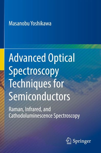
Advanced Optical Spectroscopy Techniques for Semiconductors
Raman, Infrared, and Cathodoluminescence Spectroscopy
Versandkostenfrei!
Versandfertig in 6-10 Tagen
83,99 €
inkl. MwSt.
Weitere Ausgaben:

PAYBACK Punkte
42 °P sammeln!
This book focuses on advanced optical spectroscopy techniques for the characterization of cutting-edge semiconductor materials. It covers a wide range of techniques such as Raman, infrared, photoluminescence, and cathodoluminescence (CL) spectroscopy, including an introduction to their physical fundamentals and best operating principles. Aimed at professionals working in the research and development of semiconductors and semiconductor materials, this book looks at a broad class of materials such as silicon and silicon dioxide, nano-diamond thin films, quantum dots, and gallium oxide. In additi...
This book focuses on advanced optical spectroscopy techniques for the characterization of cutting-edge semiconductor materials. It covers a wide range of techniques such as Raman, infrared, photoluminescence, and cathodoluminescence (CL) spectroscopy, including an introduction to their physical fundamentals and best operating principles. Aimed at professionals working in the research and development of semiconductors and semiconductor materials, this book looks at a broad class of materials such as silicon and silicon dioxide, nano-diamond thin films, quantum dots, and gallium oxide. In addition to the spectroscopic techniques covered, this book features a chapter devoted to the use of a scanning electron transmission microscope as an excitation source for CL spectroscopy. Written by a practicing industry expert in the field, this book is an ideal source of reference and best-practices guide for physicists, as well as materials scientists and engineers involved in the area of spectroscopy of semiconductor materials. Further, this book introduces the cutting-edge spectroscopy such as optical photothermal IR and Raman spectroscopy or terahertz time-domain spectroscopy (THz-TDS) etc.


