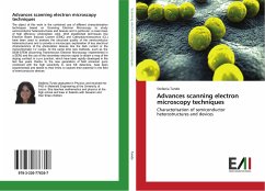
The object of this work is the combined use of different characterisation techniques based on Scanning Electron Microscopy to study semiconductor heterostructures and devices and in particular, a novel class of high efficiency photovoltaic cells. Well established techniques like Electron Beam Induced Current (EBIC) and Cathodoluminescence (CL) have been used to analyse the structural quality of the semiconductor heterostructures and to provide a microscopic explanation of key electrical characteristics of the photovoltaic devices like the dark current or the monochromatic I-V curves. At the same time new methods, such as the SEM-STEM (Scanning Transmission Electron Microscopy implemented in a SEM) and the use of the secondary electron signal to obtain a map of the doping contrast in a p-n junction, which have been rapidly developed in the last few years thanks to the new generation of field emission guns combined with the high sensitivity in- lens SE detectors, have been experimented and tested to their limits to explore their potential in the field of semiconductor devices.
Hinweis: Dieser Artikel kann nur an eine deutsche Lieferadresse ausgeliefert werden.
Hinweis: Dieser Artikel kann nur an eine deutsche Lieferadresse ausgeliefert werden.

