AlGaN/GaN HEMTs Reliability. Degradation Modes and Analysis

PAYBACK Punkte
0 °P sammeln!
AlGaN/GaN HEMTs reliability and stability issues were investigated in dependence on epitaxial design and process modification. DC-Step-Stress-Tests have been performed on wafers as a fast device robustness screening method. As a criterion of robustness they deliver a critical source-drain voltage for the onset of degradation. Several degradation modes were observed which depend on epi design, epi quality and process technology. Electrical and optical characterizations together with electric field simulations were performed to get insight into respective degradation modes. It has been found tha...
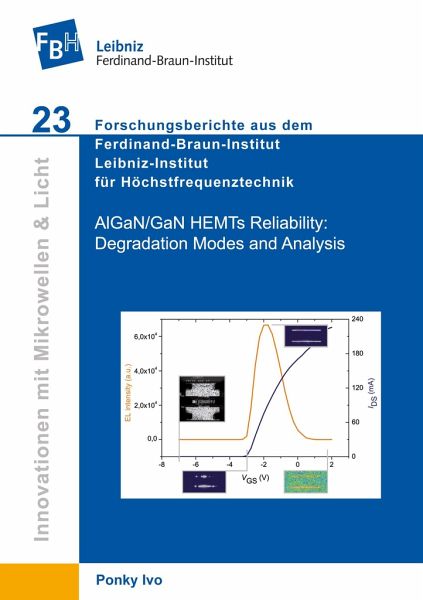
AlGaN/GaN HEMTs reliability and stability issues were investigated in dependence on epitaxial design and process modification. DC-Step-Stress-Tests have been performed on wafers as a fast device robustness screening method. As a criterion of robustness they deliver a critical source-drain voltage for the onset of degradation. Several degradation modes were observed which depend on epi design, epi quality and process technology. Electrical and optical characterizations together with electric field simulations were performed to get insight into respective degradation modes. It has been found that AlGaN/GaN HEMT devices with GaN cap show higher critical source-drain voltages as compared to non-capped devices. Devices with low Al concentration in the AlGaN barrier layer also show higher critical source-drain voltages. Superior stability and robustness performance have been achieved from devices with AlGaN backbarrier epi design grown on n-type SiC substrate. For the onset on any degradation modes the presence of high electrical fields is most decisive for ON- and OFF-state operation conditions. Therefore careful epi design to reduce high electric field is mandatory. It is also shown that epi buffer quality and growth process have a great impact on device robustness. Defects such as point defects and dislocations are assumed to be created initially during stressing and accumulated to larger defect clusters during device stressing. Electroluminescence (EL) measurements were performed to detect early degradation. Extended localized defects are resulting as bright spots at OFF-state conditions in conjunction with a gate leakage increase.


