Kazuo Morigaki, Sandor Kugler, Koichi Shimakawa
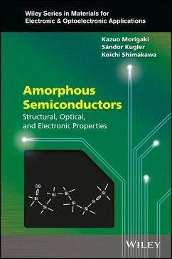
Amorphous Semiconductors
Structural, Optical, and Electronic Properties
Kazuo Morigaki, Sandor Kugler, Koichi Shimakawa
Amorphous Semiconductors
Structural, Optical, and Electronic Properties
- Gebundenes Buch
- Merkliste
- Auf die Merkliste
- Bewerten Bewerten
- Teilen
- Produkt teilen
- Produkterinnerung
- Produkterinnerung
Amorphous semiconductors are subtances in the amorphous solid state that have the properties of a semiconductor and which are either covalent or tetrahedrally bonded amorphous semiconductors or chelcogenide glasses. _ Developed from both a theoretical and experimental viewpoint _ Deals with, amongst others, preparation techniques, structural, optical and electronic properties, and light induced phenomena _ Explores different types of amorphous semiconductors including amorphous silicon, amorphous semiconducting oxides and chalcogenide glasses _ Applications include solar cells, thin film…mehr
Andere Kunden interessierten sich auch für
![Organic Semiconductors for Optoelectronics Organic Semiconductors for Optoelectronics]() Organic Semiconductors for Optoelectronics209,99 €
Organic Semiconductors for Optoelectronics209,99 €![Group III-Nitride Semiconductor Optoelectronics Group III-Nitride Semiconductor Optoelectronics]() C. Jayant PraharajGroup III-Nitride Semiconductor Optoelectronics139,99 €
C. Jayant PraharajGroup III-Nitride Semiconductor Optoelectronics139,99 €![Metal Oxide Semiconductors Metal Oxide Semiconductors]() Zhigang ZangMetal Oxide Semiconductors97,99 €
Zhigang ZangMetal Oxide Semiconductors97,99 €![Thermal Management Materials for Electronic Packaging Thermal Management Materials for Electronic Packaging]() Thermal Management Materials for Electronic Packaging104,99 €
Thermal Management Materials for Electronic Packaging104,99 €![Lead-Free Solders Lead-Free Solders]() Lead-Free Solders186,99 €
Lead-Free Solders186,99 €![Flexible Electronic Packaging and Encapsulation Technology Flexible Electronic Packaging and Encapsulation Technology]() Flexible Electronic Packaging and Encapsulation Technology105,99 €
Flexible Electronic Packaging and Encapsulation Technology105,99 €![3D and Circuit Integration of MEMS 3D and Circuit Integration of MEMS]() Masayoshi Esashi3D and Circuit Integration of MEMS119,99 €
Masayoshi Esashi3D and Circuit Integration of MEMS119,99 €-
-
-
Amorphous semiconductors are subtances in the amorphous solid state that have the properties of a semiconductor and which are either covalent or tetrahedrally bonded amorphous semiconductors or chelcogenide glasses.
_ Developed from both a theoretical and experimental viewpoint
_ Deals with, amongst others, preparation techniques, structural, optical and electronic properties, and light induced phenomena
_ Explores different types of amorphous semiconductors including amorphous silicon, amorphous semiconducting oxides and chalcogenide glasses
_ Applications include solar cells, thin film transistors, sensors, optical memory devices and flat screen devices including televisions
Hinweis: Dieser Artikel kann nur an eine deutsche Lieferadresse ausgeliefert werden.
Produktdetails
- Produktdetails
- Wiley Series in Materials for Electronic & Optoelectronic Applications
- Verlag: Wiley & Sons
- Artikelnr. des Verlages: 1W118757920
- 1. Auflage
- Seitenzahl: 286
- Erscheinungstermin: 6. März 2017
- Englisch
- Abmessung: 231mm x 157mm x 20mm
- Gewicht: 544g
- ISBN-13: 9781118757925
- ISBN-10: 1118757920
- Artikelnr.: 47114764
- Herstellerkennzeichnung
- Libri GmbH
- Europaallee 1
- 36244 Bad Hersfeld
- gpsr@libri.de
Kazuo Morigaki, Professor Emeritus, University of Tokyo. Morigaki received his Ph.D. degree in physics from Osaka University in 1959. Since then, he has joined Osaka University, Sony Corporation Research Laboratory, Centre d'Etudes Nuclèares de Saclay, University of Tokyo (Institute for Solid State Physics), Yamaguchi University and Hiroshima Institute of Technology. Sandor Kugler, Associate Professor, Department of Theoretical Physics, Budapest University of Technology and Economics, Hungary. Kugler received both his degree in and his PhD in physics from ELTE, Budapest. He joined the quantum theory group, Institute of Physics, Technical University of Budapest, during 1974-1993 as research associate. Since 1993, he has been Associate Professor. Koichi Shimakawa, Professor Emeritus and Fellow, Gifu University, Japan. Shimakawa received his PhD from Nagoya University in 1975. Since then, he has been at Gifu University, becoming Professor in the period 1989-2008. He retired from Gifu University in 2008, and is senior researcher, Nagoya Industrial Science Institute, Nagoya, and visiting Professor, Department of Chemistry, University of Pardubice, Czech Republic.
Series Preface xi
Preface xiii
1 Introduction 1
1.1 General Aspects of Amorphous Semiconductors 1
1.2 Chalcogenide Glasses 3
1.3 Applications of Amorphous Semiconductors 3
References 3
2 Preparation Techniques 5
2.1 Growth of a-Si:H Films 5
2.1.1 PECVD Technique 5
2.1.2 HWCVD Technique 6
2.2 Growth of Amorphous Chalcogenides 6
References 8
3 Structural Properties of Amorphous Silicon and Amorphous Chalcogenides 11
3.1 General Aspects 11
3.1.1 Definitions of Crystalline and Noncrystalline 11
3.2 Optical Spectroscopy 12
3.2.1 Raman Scattering 12
3.2.2 Infrared Absorption 13
3.3 Neutron Diffraction 15
3.3.1 Diffraction Measurements on Amorphous Silicon 17
3.3.2 Diffraction Measurements on Hydrogenated Amorphous Silicon 18
3.3.3 Diffraction Measurements on Amorphous Germanium 19
3.3.4 Diffraction Measurements on Amorphous Selenium 19
3.4 Computer Simulations 20
3.4.1 Monte Carlo-Type Methods for Structure Derivation 20
3.4.2 Atomic Interactions 21
3.4.3 a-Si Models Constructed by Monte Carlo Simulation 25
3.4.4 Reverse Monte Carlo Methods 26
3.4.5 a-Si Model Constructed by RMC Simulation 28
3.4.6 a-Se Model Constructed by RMC Simulation 30
3.4.7 Molecular Dynamics Simulation 32
3.4.8 a-Si Model Construction by Molecular Dynamics Simulation 34
3.4.9 a-Si:H Model Construction by Molecular Dynamics Simulation 34
3.4.10 a-Se Model Construction by Molecular Dynamics Simulation 35
3.4.11 Car and Parrinello Method 38
References 38
4 Electronic Structure of Amorphous Semiconductors 43
4.1 Bonding Structures 43
4.1.1 Bonding Structures in Column IV Elements 44
4.1.2 Bonding Structures in Column VI Elements 45
4.2 Electronic Structure of Amorphous Semiconductors 46
4.3 Fermi Energy of Amorphous Semiconductors 47
4.4 Differences between Amorphous and Crystalline Semiconductors 49
4.5 Charge Distribution in Pure Amorphous Semiconductors 49
4.6 Density of States in Pure Amorphous Semiconductors 52
4.7 Dangling Bonds 54
4.8 Doping 57
References 58
5 Electronic and Optical Properties of Amorphous Silicon 61
5.1 Introduction 61
5.2 Band Tails and Structural Defects 62
5.2.1 Introduction 62
5.2.2 Band Tails 62
5.2.3 Structural Defects 66
5.3 Recombination Processes 68
5.3.1 Introduction 68
5.3.2 Radiative Recombination 68
5.3.3 Nonradiative Recombination 70
5.3.4 Recombination Processes and Recombination Centers in a-Si:H 72
5.3.5 Spin-Dependent Recombination 73
5.4 Electrical Properties 74
5.4.1 DC Conduction 74
5.4.2 AC Conduction 80
5.4.3 Hall Effect 87
5.4.4 Thermoelectric Power 88
5.4.5 Doping Effect 89
5.5 Optical Properties 92
5.5.1 Fundamental Optical Absorption 92
5.5.2 Weak Absorption 94
5.5.3 Photoluminescence 96
5.5.4 Frequency-Resolved Spectroscopy (FRS) 96
5.5.5 Photoconductivity 101
5.5.6 Dispersive Photoconduction 109
5.6 Electron Magnetic Resonance and Spin-Dependent Properties 112
5.6.1 Introduction 112
5.6.2 Electron Magnetic Resonance 112
5.6.3 Spin-Dependent Properties 128
5.7 Light-Induced Phenomena and Light-Induced Defect Creatio

