At the end of the Second World War, a new technological trend was born: integrated electronics. This trend relied on the enormous rise of integrable electronic devices. Analog Devices and Circuits is composed of two volumes: the first deals with analog components, and the second with associated analog circuits. The goal here is not to create an overly comprehensive analysis, but rather to break it down into smaller sections, thus highlighting the complexity and breadth of the field. This first volume, after a brief history, describes the two main devices, namely bipolar transistors and MOS,…mehr
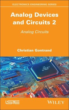
At the end of the Second World War, a new technological trend was born: integrated electronics. This trend relied on the enormous rise of integrable electronic devices. Analog Devices and Circuits is composed of two volumes: the first deals with analog components, and the second with associated analog circuits. The goal here is not to create an overly comprehensive analysis, but rather to break it down into smaller sections, thus highlighting the complexity and breadth of the field. This first volume, after a brief history, describes the two main devices, namely bipolar transistors and MOS, with particular importance given to the modeling aspect. In doing so, we deal with new devices dedicated to radio frequency, which touches on nanoelectronics. We will also address some of the notions related to quantum mechanics. Finally, Monte Carlo methods, by essence statistics, will be introduced, which have become more and more important since the middle of the twentieth century. The second volume deals with the circuits that "use" the analog components that were introduced in Volume 1. Here, a particular emphasis is placed on the main circuit: the operational amplifier.Hinweis: Dieser Artikel kann nur an eine deutsche Lieferadresse ausgeliefert werden.
Christian Gontrand is a Professor at INL/INSA Lyon, France, focusing on 3D circuits. He was formerly a Head Professor in the Smart Power Integration team at Laboratoire Ampère and had technical charge of the CIMIRLY from 1988 to 1996. His current research focuses on Artificial Intelligence applied to health.
Inhaltsangabe
Preface ix Introduction xiii Chapter 1 Bipolar Junction Transistor 1 1.1 Introduction 1 1.1.1 A schematic technological embodiment of an integrated bipolar junction transistor 2 1.2 Transistor effect 4 1.2.1 Flows and currents 5 1.2.2 Compromises for bipolar junction transistor 6 1.2.3 Configurations and associated current gains 7 1.3 Bipolar junction transistor: some calculations 9 1.3.1 Various modes of operation 15 1.4 The NPN transistor; Ebers-Moll model (1954: Jewell James Ebers and John L Moll) 16 1.4.1 Gummel curves 18 1.4.2 Consideration of second-order effects for the static model 19 1.4.3 Early curves 20 1.4.4 Base width modulation; Early effect 20 1.4.5 Ebers-Moll model wide signals 22 1.4.6 Current gain 26 1.5 Simple bipolar junction transistor model 27 1.6 Network of static characteristics of the bipolar junction transistor 27 1.6.1 Common emitter configuration 31 1.6.2 Common emitter configuration with emitter degeneration 34 1.7 Some applications 35 1.7.1 Current mirrors 35 1.7.2 Differential pair 38 1.7.3 Output stage 41 1.8 Application: operational amplifier 43 1.9 BiCMOS 43 Chapter 2 Mosfet 45 2.1 Introduction 45 2.1.1 Base structure 45 2.1.2 Working principle 46 2.2 MOS capability: electric model and curve C(V) 47 2.3 Different types of MOS transistors 49 2.4 A CMOS technological process 50 2.5 Electric modeling of the NMOS enhancement transistor 52 2.6 Off state 52 2.7 Linear or ohmic or unsaturated regime 52 2.7.1 Saturation regime 53 2.7.2 High saturation velocity 53 2.7.3 Static characteristics 54 2.8 Applications 56 2.8.1 Digital inverter 56 2.8.2 Active resistor 58 2.8.3 MOS Single current mirror 59 2.8.4 MOS differential amplifier 60 2.9 Explained technological steps of a CMOS 60 Chapter 3 Devices Dedicated to Radio Frequency: Toward Nanoelectronics 75 3.1 Introduction 75 3.2 Model for HBT SiGeC and device structure 76 3.2.1 Modeling the drift-diffusion equation 76 3.3 MOS of the future? 83 3.3.1 Introduction 83 3.3.2 Dgmos 84 3.3.3 Transport in nanoscale MOSFETs 85 3.3.4 Numerical methods 87 3.4 Conclusion 111 3.5 MATLAB use 112 3.5.1 Computer-aided modelling and simulations: synopsis 112 3.5.2 Calculation of the second elementary member ¿ 1 139 3.6 Conclusion 185 Appendix 187 References 211 Index 213
Es gelten unsere Allgemeinen Geschäftsbedingungen: www.buecher.de/agb
Impressum
www.buecher.de ist ein Internetauftritt der buecher.de internetstores GmbH
Geschäftsführung: Monica Sawhney | Roland Kölbl | Günter Hilger
Sitz der Gesellschaft: Batheyer Straße 115 - 117, 58099 Hagen
Postanschrift: Bürgermeister-Wegele-Str. 12, 86167 Augsburg
Amtsgericht Hagen HRB 13257
Steuernummer: 321/5800/1497
USt-IdNr: DE450055826