Thorsten Lill
Atomic Layer Processing
Thorsten Lill
Atomic Layer Processing
- Broschiertes Buch
- Merkliste
- Auf die Merkliste
- Bewerten Bewerten
- Teilen
- Produkt teilen
- Produkterinnerung
- Produkterinnerung
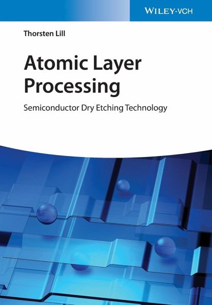
This practical guide, written by an author actively involved in corporate R&D, provides in-depth information on etching technologies that are used in the semiconductor industry, helping engineers to select the right technologies for their task and to design etching processes.
Andere Kunden interessierten sich auch für
- Handbook of Self-Cleaning Surfaces and Materials227,99 €
- Inkjet Printing in Industry499,00 €
- Haihui WangMXene Membranes for Separations139,00 €
- Printable Mesoscopic Perovskite Solar Cells105,99 €
- Lingwei MaSmart Protective Coatings for Corrosion Control129,99 €
- Functional Materials from Colloidal Self-assembly235,34 €
- Emmanuel Defa˙Integration of Ferroelectric and Piezoelectric Thin Films251,99 €
-
-
-
This practical guide, written by an author actively involved in corporate R&D, provides in-depth information on etching technologies that are used in the semiconductor industry, helping engineers to select the right technologies for their task and to design etching processes.
Produktdetails
- Produktdetails
- Verlag: Wiley-VCH
- Artikelnr. des Verlages: 1134668 000
- 1. Auflage
- Seitenzahl: 300
- Erscheinungstermin: 19. April 2021
- Englisch
- Abmessung: 244mm x 170mm x 16mm
- Gewicht: 584g
- ISBN-13: 9783527346684
- ISBN-10: 3527346686
- Artikelnr.: 60093503
- Herstellerkennzeichnung
- Wiley-VCH GmbH
- Boschstr. 12
- 69469 Weinheim
- wiley.buha@zeitfracht.de
- www.wiley-vch.de
- +49 (06201) 606-0 (AB ab 18.00 Uhr)
Thorsten Lill is a Vice President for Emerging Etch Technologies and Systems at Lam Research, the market leader in etching tools for the semiconductor industry. He has been working in the field of plasma, radical, thermal, ion beam and plasma etching since 1995. He has a Ph.D. in Physics from the Albert-Ludwigs-University in Freiburg, Germany and was a post doc at the Argonne National Laboratory. He has a track record in developing commercially successful etching equipment for the semiconductor industry. He published 85 articles and 66 patents in the field. Thorsten Lill holds a certificate in Entrepreneurship and Innovation from Stanford University.
1. INTRODUCTION
2. FUNDAMENTALS
2.1. Important performance metrics of etching processes
2.2. Physisorption and Chemisorption
2.3. Desorption
2.4. Surface Reactions
2.5. Sputtering
2.6. Implantation
2.7. Diffusion
2.8. Transport phenomena in 3D features
2.8.1. Neutral transport
2.8.2. Ion transport
2.8.3. Transport of reaction products
2.9. Classification of etching technologies
3. THERMAL ETCHING
3.1. Mechanism and performance metrics of Thermal Etching
3.2. Applications examples
4. THERMAL ISOTROPIC ALE
4.1. Mechanism of Thermal Isotropic ALE
4.1.1. Chelation / Condensation ALE
4.1.2. Ligand Exchange ALE
4.1.3. Conversion ALE
4.1.4. Oxidation / Fluorination ALE
4.2. Performance metrics of Thermal Isotropic ALE
4.3. Plasma-assisted Isotropic ALE
4.4. Applications examples
4.4.1. Area-selective deposition
4.4.2. Formation of lateral devices
5. RADICAL ETCHING
5.1. Mechanism of Radical Etching
5.2. Performance metrics
5.3. Applications examples
6. DIRECTIONAL ALE
6.1. Mechanism of Directional ALE
6.1.1. ALE with directional modification step
6.1.2. ALE with directional removal step and modification by chemisorption and diffusion
6.1.3. ALE with directional removal step and modification by reactive layer deposition
6.2. Performance metrics
6.3. Applications examples
7. REACTIVE ION ETCHING
7.1. Reactive Ion Etching Mechanisms
7.1.1. Simultaneous species fluxes
7.1.2. Chemical sputtering
7.1.3. Mixed layer formation
7.1.4. Role of etching products
7.2. Performance metrics
7.3. Application examples
7.3.1. Patterning
7.3.2. Logic Devices
7.3.3. DRAM and 3D NAND memory
7.3.4. Emerging memories
8. ION BEAM ETCHING
8.1. Mechanism and performance metrics of Ion Beam Etching
8.2. Applications examples
9. ETCHING SPECIES GENERATION
9.1. Introduction of low temperature plasmas
9.2. Capacitively coupled plasmas
9.3. Inductively coupled plasmas
9.4. Ion energy distribution modulation
9.5. Plasma-pulsing
9.6. Grid sources
10. EMERGING ETCHING TECHNOLOGIES
10.1. Electron assisted chemical etching
10.2. Photon assisted chemical etching