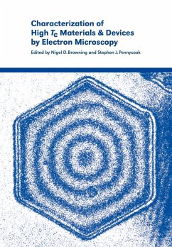
A comprehensive account of the application of electron-based microscopies to the study of high-Tc superconductors.
This is a clear account of the application of electron-based microscopies to the study of high-Tc superconductors. Written by leading experts, this compilation provides a comprehensive review of scanning electron microscopy, transmission electron microscopy and scanning transmission electron microscopy, together with details of each technique and its applications. Introductory chapters cover the basics of high-resolution transmission electron microscopy, including a chapter devoted to specimen preparation techniques, and microanalysis by scanning transmission electron microscopy. Ensuing chapters examine identification of superconducting compounds, imaging of superconducting properties by low-temperature scanning electron microscopy, imaging of vortices by electron holography and electronic structure determination by electron energy loss spectroscopy. The use of scanning tunnelling microscopy for exploring surface morphology, growth processes and the mapping of superconducting carrier distributions is discussed. Final chapters consider applications of electron microscopy to the analysis of grain boundaries, thin films and device structures. Detailed references are included.
Review quote:
'- a useful and nearly comprehensive guide to current work in the subject.' J. P. Davey, Contemporary Physics
Table of contents:
List of contributors; Preface; 1. High-resolution transmission electron microscopy S. Horiuchi and L. He; 2. Holography in the transmission electron microscope A. Tonomura; 3. Microanalysis by scanning transmission electron microscopy L. M. Brown and J. Yuan; 4. Specimen preparation for transmission electron microscopy J. G. Wen; 5. Low-temperature scanning electron microscopy R. P. Huebener; 6. Scanning tunneling microscopy M. E. Hawley; 7. Identification of new superconducting compounds by electron microscopy G. Van Tendeloo and T. Krekels; 8. Valence band electron energy loss spectroscopy (EELS) of oxide superconductors Y. Y. Wang and V. P. Dravid; 9. Investigation of charge distribution in Bi2Sr2CaCu2O8 and YBa2Cu3O7 Y. Zhu; 10. Grain boundaries in high Tc materials: transport properties and structure K. L. Merkle, Y. Gao and B. V. Vuchic; 11. The atomic structure and carrier concentration at grain boundaries in YBa2Cu3O7-d N. D. Browning, M. F. Chisholm and S. J. Pennycook; 12. Microstructures in superconducting YBa2Cu3O7 thin films A. F. Marshall; 13. Investigations on the microstructure of YBa2Cu3O7 thin-film edge Josephson junctions by high-resolution electron microscopy C. L. Jia and K. Urban; 14. Controlling the structure and properties of high Tc thin-film devices E. Olsson.
Hinweis: Dieser Artikel kann nur an eine deutsche Lieferadresse ausgeliefert werden.

