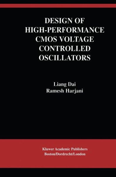
Design of High-Performance CMOS Voltage-Controlled Oscillators
Versandkostenfrei!
Versandfertig in 6-10 Tagen
113,99 €
inkl. MwSt.
Weitere Ausgaben:

PAYBACK Punkte
57 °P sammeln!
Design of High-Performance CMOS Voltage-Controlled Oscillators presents a phase noise modeling framework for CMOS ring oscillators. The analysis considers both linear and nonlinear operation. It indicates that fast rail-to-rail switching has to be achieved to minimize phase noise. Additionally, in conventional design the flicker noise in the bias circuit can potentially dominate the phase noise at low offset frequencies. Therefore, for narrow bandwidth PLLs, noise up conversion for the bias circuits should be minimized. We define the effective Q factor (Qeff) for ring oscillators and predict i...
Design of High-Performance CMOS Voltage-Controlled Oscillators presents a phase noise modeling framework for CMOS ring oscillators. The analysis considers both linear and nonlinear operation. It indicates that fast rail-to-rail switching has to be achieved to minimize phase noise. Additionally, in conventional design the flicker noise in the bias circuit can potentially dominate the phase noise at low offset frequencies. Therefore, for narrow bandwidth PLLs, noise up conversion for the bias circuits should be minimized. We define the effective Q factor (Qeff) for ring oscillators and predict its increase for CMOS processes with smaller feature sizes. Our phase noise analysis is validated via simulation and measurement results.
The digital switching noise coupled through the power supply and substrate is usually the dominant source of clock jitter. Improving the supply and substrate noise immunity of a PLL is a challenging job in hostile environments such as a microprocessor chip where millions of digital gates are present.
The digital switching noise coupled through the power supply and substrate is usually the dominant source of clock jitter. Improving the supply and substrate noise immunity of a PLL is a challenging job in hostile environments such as a microprocessor chip where millions of digital gates are present.


