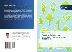
Energy deficiency is most serious problem of the world and practical use as well as role of semiconducting materials in photovoltaic technology is discussed. How all properties of as grown semiconductor can be alter in such way to achieve optimum solar cell efficiency, is also analyzed. General bottom up and top down approach for synthesis of semiconducting nanoparticles is given in detail. Electrical and Dielectric characterization of as synthesized Tin Selenide nanoparticles is presented. Electrical and Dielectric properties changes as a function of synthesis temperature of pure Tin Selenide and doping level of copper concentration also. Such properties is studied when materials dimensions are reduces to nanometer is also explained with the help of theoretical physics. Energy of activation for pure and copper doped SnSe semiconducting nanoparticles is explained with the help of mathematics and concepts of physics behind that mathematics. How and why size of nanoparticles plays important role in altering the properties of material is also discussed in depth.
Bitte wählen Sie Ihr Anliegen aus.
Rechnungen
Retourenschein anfordern
Bestellstatus
Storno

