74,99 €
inkl. MwSt.
Versandkostenfrei*
Versandfertig in 6-10 Tagen
payback
37 °P sammeln
  • Gebundenes Buch

Semiconductor quantum optics is on the verge of moving from the lab to real world applications. When stepping from basic research to new technologies, device engineers will need new simulation tools for the design and optimization of quantum light sources, which combine classical device physics with cavity quantum electrodynamics. This thesis aims to provide a holistic description of single-photon emitting diodes by bridging the gap between microscopic and macroscopic modeling approaches. The central result is a novel hybrid quantum-classical model system that self-consistently couples…mehr

Produktbeschreibung
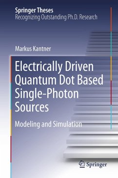
Semiconductor quantum optics is on the verge of moving from the lab to real world applications. When stepping from basic research to new technologies, device engineers will need new simulation tools for the design and optimization of quantum light sources, which combine classical device physics with cavity quantum electrodynamics. This thesis aims to provide a holistic description of single-photon emitting diodes by bridging the gap between microscopic and macroscopic modeling approaches. The central result is a novel hybrid quantum-classical model system that self-consistently couples semi-classical carrier transport theory with open quantum many-body systems. This allows for a comprehensive description of quantum light emitting diodes on multiple scales: It enables the calculation of the quantum optical figures of merit together with the simulation of the spatially resolved current flow in complex, multi-dimensional semiconductor device geometries out of one box. The hybrid system isshown to be consistent with fundamental laws of (non-)equilibrium thermodynamics and is demonstrated by numerical simulations of realistic devices.
Autorenporträt
Markus Kantner has studied physics at the Humboldt University of Berlin with focus on nonlinear dynamics and complex system with time delayed feedback. He received his Bachelor of Science and Master of Science degrees in 2010 and 2013, respectively. Since 2013, he is with the Weierstrass Institute for Applied Analysis and Stochastics (WIAS) in Berlin, working on multi-physics modeling and numerical simulation of semiconductor opto-electronic devices. In 2018, Markus Kantner received the Dr. rer. nat. degree in Theoretical Physics from the Technical University Berlin. Currently, he is a post-doctoral researcher at the WIAS within the German Cluster of Excellence MATH+.