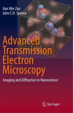
In this book, the bases of imaging and diffraction in transmission electron microscopy (TEM) and scanning transmission electron microscopy (STEM) are explained in the style of a textbook. The book focuses on the explanation of electron microscopic imaging of TEM and STEM without including in the main text distracting information on basic knowledge of crystal diffraction, wave optics, electron lens, and scattering and diffraction theories, which are explained separately in the appendices. A comprehensive explanation is provided on the basis of Fourier transform theory, and this approach is…mehr
In this book, the bases of imaging and diffraction in transmission electron microscopy (TEM) and scanning transmission electron microscopy (STEM) are explained in the style of a textbook. The book focuses on the explanation of electron microscopic imaging of TEM and STEM without including in the main text distracting information on basic knowledge of crystal diffraction, wave optics, electron lens, and scattering and diffraction theories, which are explained separately in the appendices. A comprehensive explanation is provided on the basis of Fourier transform theory, and this approach is unique in comparison with other advanced resources on high-resolution electron microscopy. With the present textbook, readers are led to understand the essence of the imaging theories of TEM and STEM without being diverted by other knowledge of electron microscopy. The up-to-date information in this book, particularly on imaging details of STEM and aberration corrections, is valuable worldwide fortoday's graduate students and professionals just starting their careers.
Dr. Nobuo Tanaka is a designated professor of Institute of Materials and Systems for Sustainability (IMaSS) of Nagoya University and an adjunct senior researcher of Japan Fine Ceramic Center (JFCC). He received a ph.D degree from Applied Physics Department of Nagoya University in 1978, and became an assistant professor of the department. He stayed Arizona State University as a visiting scholar to study with the late Prof. J. Cowley from 1983 to 1985. He was appointed a full professor of Applied Physics of Nagoya University in 1999 through an associate professor. In 2001, he moved to Center of Integrated Research for Science and Engineering (CIRSE) of Nagoya University, which was renamed EcoTopia Science Institute (ESI) in 2004. He was the director of the institute from 2012 to 2015. He is also the president of Japanese Microscopy Society (JSM) from 2015 to 2017. His professionals are high-resolution electron microscopy and nano-diffraction, and physics of atomic clusters and thin filmsas well as surfaces and interfaces of semiconductors. He is also the editor/author of a textbook as Scanning Transmission Electron Microscopy of Nanomaterials.
Inhaltsangabe
Seeing nanometer-sized world.- Structure and imaging of a transmission electron microscope (TEM).- Basic theories of TEM imaging.- Resolution and image contrast of a transmission electron microscope (TEM).- What is high-resolution transmission electron microscopy ?.- Lattice images and structure images.- Imaging theory of high-resolution TEM and image simulation.- Advanced transmission electron microscopy.- What is scanning transmission electron microscopy (STEM)?.- Imaging of scanning transmission electron microscopy (STEM).- Image contrast and its formation mechanism in STEM.- Imaging theory for STEM.- Future prospects and possibility of TEM and STEM.- Concluding remarks.- Introduction of Fourier transforms for TEM and STEM.- Imaging by using a convex lens: Convex lens as phase shifter.- Contrast transfer function of a transmission electron microscope: Key term for understanding of phase contrast in HRTEM.- Complex-valued expression of aberrations of a round lens.- Cowley's theoryfor TEM and STEM imaging.- Introduction to the imaging theory for TEM including non-linear terms.- What are image processing methods?.- Elemental analysis by electron microscopes: Analysis using an electron probe.- Electron beam damage to specimens.- Scattering of electrons by an atom: Fundamental process for visualization of a single atom by TEM.- Electron diffraction and convergent beam electron diffraction (CBED): Basis for formation of lattice fringes in TEM and image intensity of STEM.- Bethe's method for dynamical electron diffraction: Basic theory of electron diffraction in thicker crystals.- Column approximation and Howie-Whelan's method for dynamical electron diffraction: Theory for observation of lattice defects.- Van-Dyck's method for dynamical electron diffraction and imaging: Basis of atomic column imaging.- Eikonal theory for scattering of electrons by a potential.- Debye-Waller factor and thermal diffuse scattering (TDS).- Relativistic effects to diffraction and imagingby a transmission electron microscope: Basic theories for high-voltage electron microscopy.
Rezensionen
"I enjoyed reading this book. It covers a wide range of applications, from basics on electron microscopy and diffraction, to more advanced, newly developed techniques for imaging and diffraction. ... I strongly recommend this book as a resource for electron microscopists with a basic knowledge of TEM and STEM who are interested in advanced imaging and diffraction techniques." (Lourdes Salamanca-Riba, MRS Bulletin, Vol. 43, May, 2018)
Es gelten unsere Allgemeinen Geschäftsbedingungen: www.buecher.de/agb
Impressum
www.buecher.de ist ein Internetauftritt der buecher.de internetstores GmbH
Geschäftsführung: Monica Sawhney | Roland Kölbl | Günter Hilger
Sitz der Gesellschaft: Batheyer Straße 115 - 117, 58099 Hagen
Postanschrift: Bürgermeister-Wegele-Str. 12, 86167 Augsburg
Amtsgericht Hagen HRB 13257
Steuernummer: 321/5800/1497