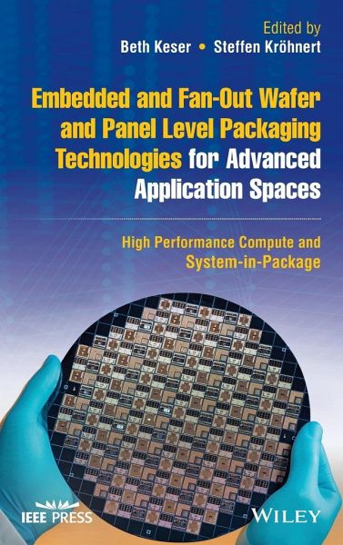
Embedded and Fan-Out Wafer and Panel Level Packaging Technologies for Advanced Application Spaces
High Performance Compute and System-In-Package
Herausgegeben: Keser, Beth; Kröhnert, Steffen
Versandkostenfrei!
Versandfertig in über 4 Wochen
134,99 €
inkl. MwSt.
Weitere Ausgaben:

PAYBACK Punkte
67 °P sammeln!
Discover an up-to-date exploration of Embedded and Fan-Out Waver and Panel Level technologiesIn Embedded and Fan-Out Wafer and Panel Level Packaging Technologies for Advanced Application Spaces: High Performance Compute and System-in-Package, a team of accomplished semiconductor experts delivers an in-depth treatment of various fan-out and embedded die approaches.The book begins with a market analysis of the latest technology trends in Fan-Out and Wafer Level Packaging before moving on to a cost analysis of these solutions. The contributors discuss the new package types for advanced applicatio...
Discover an up-to-date exploration of Embedded and Fan-Out Waver and Panel Level technologies
In Embedded and Fan-Out Wafer and Panel Level Packaging Technologies for Advanced Application Spaces: High Performance Compute and System-in-Package, a team of accomplished semiconductor experts delivers an in-depth treatment of various fan-out and embedded die approaches.
The book begins with a market analysis of the latest technology trends in Fan-Out and Wafer Level Packaging before moving on to a cost analysis of these solutions. The contributors discuss the new package types for advanced application spaces being created by companies like TSMC, Deca Technologies, and ASE Group. Finally, emerging technologies from academia are explored.
Embedded and Fan-Out Wafer and Panel Level Packaging Technologies for Advanced Application Spaces is an indispensable resource for microelectronic package engineers, managers, and decision makers working with OEMs and IDMs. It is also a must-read for professors and graduate students working in microelectronics packaging research.


