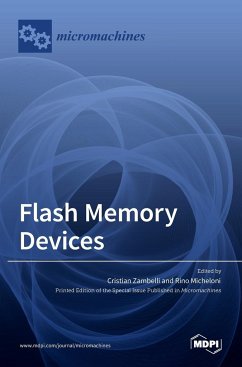
Flash memory devices have represented a breakthrough in storage since their inception in the mid-1980s, and innovation is still ongoing. The peculiarity of such technology is an inherent flexibility in terms of performance and integration density according to the architecture devised for integration. The NOR Flash technology is still the workhorse of many code storage applications in the embedded world, ranging from microcontrollers for automotive environment to IoT smart devices. Their usage is also forecasted to be fundamental in emerging AI edge scenario. On the contrary, when massive data storage is required, NAND Flash memories are necessary to have in a system. You can find NAND Flash in USB sticks, cards, but most of all in Solid-State Drives (SSDs). Since SSDs are extremely demanding in terms of storage capacity, they fueled a new wave of innovation, namely the 3D architecture. Today "3D" means that multiple layers of memory cells are manufactured within the same piece of silicon, easily reaching a terabit capacity. So far, Flash architectures have always been based on "floating gate," where the information is stored by injecting electrons in a piece of polysilicon surrounded by oxide. On the contrary, emerging concepts are based on "charge trap" cells. In summary, flash memory devices represent the largest landscape of storage devices, and we expect more advancements in the coming years. This will require a lot of innovation in process technology, materials, circuit design, flash management algorithms, Error Correction Code and, finally, system co-design for new applications such as AI and security enforcement.
Hinweis: Dieser Artikel kann nur an eine deutsche Lieferadresse ausgeliefert werden.
Hinweis: Dieser Artikel kann nur an eine deutsche Lieferadresse ausgeliefert werden.

