- Gebundenes Buch
- Merkliste
- Auf die Merkliste
- Bewerten Bewerten
- Teilen
- Produkt teilen
- Produkterinnerung
- Produkterinnerung
The fabrication of an integrated circuit requires a variety of physical and chemical processes to be performed on a semiconductor substrate. In general, these processes fall into three categories: film deposition, patterning, and semiconductor doping. Films of both conductors and insulators are used to connect and isolate transistors and their components.
By creating structures of these various components millions of transistors can be built and wired together to form the complex circuitry of modern microelectronic devices. Fundamental to all of these processes is lithography, ie, the…mehr
Andere Kunden interessierten sich auch für
- Chris MackFundamental Principles of Optical77,99 €
- Quan LiSelf-Organized Organic Semiconductors158,99 €
- Eishi H. IbeTerrestrial Radiation Effects in ULSI Devices and Electronic Systems174,99 €
- Imin CaoWafer Manufacturing180,99 €
- Sadao AdachiProperties of Semiconductor Alloys302,99 €
- Tak-Kei LamBoolean Circuit Rewiring167,99 €
- Kevin F. BrennanTheory of Modern Electronic Semiconductor Devices214,99 €
-
-
-
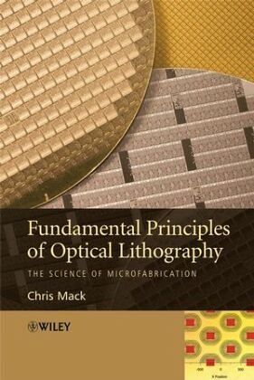
The fabrication of an integrated circuit requires a variety of physical and chemical processes to be performed on a semiconductor substrate. In general, these processes fall into three categories: film deposition, patterning, and semiconductor doping. Films of both conductors and insulators are used to connect and isolate transistors and their components.
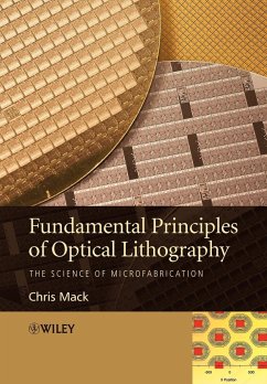
By creating structures of these various components millions of transistors can be built and wired together to form the complex circuitry of modern microelectronic devices. Fundamental to all of these processes is lithography, ie, the formation of three-dimensional relief images on the substrate for subsequent transfer of the pattern to the substrate.
This book presents a complete theoretical and practical treatment of the topic of lithography for both students and researchers. It comprises ten detailed chapters plus three appendices with problems provided at the end of each chapter.
Hinweis: Dieser Artikel kann nur an eine deutsche Lieferadresse ausgeliefert werden.
By creating structures of these various components millions of transistors can be built and wired together to form the complex circuitry of modern microelectronic devices. Fundamental to all of these processes is lithography, ie, the formation of three-dimensional relief images on the substrate for subsequent transfer of the pattern to the substrate.
This book presents a complete theoretical and practical treatment of the topic of lithography for both students and researchers. It comprises ten detailed chapters plus three appendices with problems provided at the end of each chapter.
Hinweis: Dieser Artikel kann nur an eine deutsche Lieferadresse ausgeliefert werden.
Produktdetails
- Produktdetails
- Verlag: Wiley & Sons
- 1. Auflage
- Seitenzahl: 544
- Erscheinungstermin: 1. Februar 2008
- Englisch
- Abmessung: 248mm x 177mm x 37mm
- Gewicht: 1165g
- ISBN-13: 9780470018934
- ISBN-10: 0470018933
- Artikelnr.: 23046138
- Herstellerkennzeichnung
- Libri GmbH
- Europaallee 1
- 36244 Bad Hersfeld
- 06621 890
Dr. Chris A. Mack developed the lithography simulation software PROLITH, and founded and ran the company FINLE Technologies fro ten years. He then served as Vice President of Lithography Technology for KLA-Tencor for five years, until 2005. In 2003 he received the SEMI Award for North America for his efforts in lithography simulation and education. He is also an adjunct faculty member at the University of Texas at Austin. Currently, he writes, teaches, and consults on the field of semiconductor microlithography in Austin, Texas.
Preface xv
1. Introduction to Semiconductor Lithography 1
1.1 Basics of IC Fabrication 2
1.1.1 Patterning 2
1.1.2 Etching 3
1.1.3 Ion Implantation 5
1.1.4 Process Integration 6
1.2 Moore's Law and the Semiconductor Industry 7
1.3 Lithography Processing 12
1.3.1 Substrate Preparation 14
1.3.2 Photoresist Coating 15
1.3.3 Post-Apply Bake 18
1.3.4 Alignment and Exposure 19
1.3.5 Post-exposure Bake 23
1.3.6 Development 24
1.3.7 Postbake 25
1.3.8 Measure and Inspect 25
1.3.9 Pattern Transfer 25
1.3.10 Strip 26
Problems 26
2. Aerial Image Formation - The Basics 29
2.1 Mathematical Description of Light 29
2.1.1 Maxwell's Equations and the Wave Equation 30
2.1.2 General Harmonic Fields and the Plane Wave in a Nonabsorbing Medium
32
2.1.3 Phasors and Wave Propagation in an Absorbing Medium 33
2.1.4 Intensity and the Poynting Vector 36
2.1.5 Intensity and Absorbed Electromagnetic Energy 37
2.2 Basic Imaging Theory 38
2.2.1 Diffraction 39
2.2.2 Fourier Transform Pairs 43
2.2.3 Imaging Lens 45
2.2.4 Forming an Image 47
2.2.5 Imaging Example: Dense Array of Lines and Spaces 48
2.2.6 Imaging Example: Isolated Space 50
2.2.7 The Point Spread Function 51
2.2.8 Reduction Imaging 53
2.3 Partial Coherence 56
2.3.1 Oblique Illumination 57
2.3.2 Partially Coherent Illumination 58
2.3.3 Hopkins Approach to Partial Coherence 62
2.3.4 Sum of Coherent Sources Approach 63
2.3.5 Off-Axis Illumination 65
2.3.6 Imaging Example: Dense Array of Lines and Spaces Under Annular
Illumination 66
2.3.7 Köhler Illumination 66
2.3.8 Incoherent Illumination 69
2.4 Some Imaging Examples 70
Problems 71
3. Aerial Image Formation - The Details 75
3.1 Aberrations 75
3.1.1 The Causes of Aberrations 75
3.1.2 Describing Aberrations: the Zernike Polynomial 78
3.1.3 Aberration Example - Tilt 81
3.1.4 Aberration Example - Defocus, Spherical and Astigmatism 83
3.1.5 Aberration Example - Coma 84
3.1.6 Chromatic Aberrations 85
3.1.7 Strehl Ratio 90
3.2 Pupil Filters and Lens Apodization 90
3.3 Flare 91
3.3.1 Measuring Flare 92
3.3.2 Modeling Flare 94
3.4 Defocus 95
3.4.1 Defocus as an Aberration 95
3.4.2 Defocus Example: Dense Lines and Spaces and Three-Beam Imaging 98
3.4.3 Defocus Example: Dense Lines and Spaces and Two-Beam Imaging 100
3.4.4 Image Isofocal Point 102
3.4.5 Focus Averaging 103
3.4.6 Reticle Defocus 104
3.4.7 Rayleigh Depth of Focus 105
3.5 Imaging with Scanners Versus Steppers 106
3.6 Vector Nature of Light 108
3.6.1 Describing Polarization 111
3.6.2 Polarization Example: TE Versus TM Image of Lines and Spaces 113
3.6.3 Polarization Example: The Vector PSF 114
3.6.4 Polarization Aberrations and the Jones Pupil 114
3.7 Immersion Lithography 117
3.7.1 The Optical Invariant and Hyper-NA Lithography 118
3.7.2 Immersion Lithography and the Depth of Focus 120
3.8 Image Quality 121
3.8.1 Image cd 121
3.8.2 Image Placement Error (Distortion) 123
3.8.3 Normalized Image Log-Slope (NILS) 123
3.8.4 Focus Dependence of Image Quality 125
Problems 126
4. Imaging in Resist: Standing Waves and Swing Curves 129
4.1 Standing Waves 130
4.1.1 The Nature of Standing Waves 130
4.1.2 Standing Waves for Normally Incident Light in a Single Film 131
4.1.3 Standing Waves in a Multiple-Layer Film Stack 135
4.1.4 Oblique Incidence and the Vector Nature of Light 137
4.1.5 Broadband Illumination 141
4.2 Swing Curves 144
4.2.1 Reflectivity Swing Curve 144
4.2.2 Dose-to-Clear and CD Swing Curves 148
4.2.3 Swing Curves for Partially Coherent Illumination 149
4.2.4 Swing Ratio 151
4.2.5 Effective Absorption 154
4.3 Bottom Antireflection Coatings 156
4.3.1 BARC on an Absorbing Substrate 157
4.3.2 BARCs at High Numerical Apertures 160
4.3.3 BARC on a Transparent Substrate 164
4.3.4 BARC Performance 165
4.4 Top Antireflection Coatings 167
4.5 Contrast Enhancement Layer 170
4.6 Impact of the Phase of the Substrate Reflectance 170
4.7 Imaging in Resist 173
4.7.1 Image in Resist Contrast 173
4.7.2 Calculating the Image in Resist 177
4.7.3 Resist-Induced Spherical Aberrations 179
4.7.4 Standing Wave Amplitude Ratio 181
4.8 Defining Intensity 183
4.8.1 Intensity at Oblique Incidence 183
4.8.2 Refraction into an Absorbing Material 184
4.8.3 Intensity and Absorbed Energy 187
Problems 188
5. Conventional Resists: Exposure and Bake Chemistry 191
5.1 Exposure 191
5.1.1 Absorption 191
5.1.2 Exposure Kinetics 194
5.2 Post-Apply Bake 199
5.2.1 Sensitizer Decomposition 200
5.2.2 Solvent Diffusion and Evaporation 205
5.2.3 Solvent Effects in Lithography 209
5.3 Post-exposure Bake Diffusion 210
5.4 Detailed Bake Temperature Behavior 214
5.5 Measuring the ABC Parameters 217
Problems 219
6. Chemically Amplified Resists: Exposure and Bake Chemistry 223
6.1 Exposure Reaction 223
6.2 Chemical Amplification 224
6.2.1 Amplification Reaction 225
6.2.2 Diffusion 227
6.2.3 Acid Loss 230
6.2.4 Base Quencher 232
6.2.5 Reaction-Diffusion Systems 233
6.3 Measuring Chemically Amplified Resist Parameters 235
6.4 Stochastic Modeling of Resist Chemistry 237
6.4.1 Photon Shot Noise 237
6.4.2 Chemical Concentration 239
6.4.3 Some Mathematics of Binary Random Variables 241
6.4.4 Photon Absorption and Exposure 242
6.4.5 Acid Diffusion, Conventional Resist 246
6.4.6 Acid-Catalyzed Reaction-Diffusion 247
6.4.7 Reaction-Diffusion and Polymer Deblocking 251
6.4.8 Acid-Base Quenching 253
Problems 254
7. Photoresist Development 257
7.1 Kinetics of Development 257
7.1.1 A Simple Kinetic Development Model 258
7.1.2 Other Development Models 261
7.1.3 Molecular Weight Distributions and the Critical Ionization Model 264
7.1.4 Surface Inhibition 265
7.1.5 Extension to Negative Resists 267
7.1.6 Developer Temperature 267
7.1.7 Developer Normality 268
7.2 The Development Contrast 270
7.2.1 Defining Photoresist Contrast 270
7.2.2 Comparing Definitions of Contrast 274
7.2.3 The Practical Contrast 276
7.2.4 Relationship between g and r max /r min 277
7.3 The Development Path 278
7.3.1 The Euler-Lagrange Equation 279
7.3.2 The Case of No z-Dependence 280
7.3.3 The Case of a Separable Development Rate Function 282
7.3.4 Resist Sidewall Angle 283
7.3.5 The Case of Constant Development Gradients 284
7.3.6 Segmented Development and the Lumped Parameter Model (LPM) 286
7.3.7 LPM Example - Gaussian Image 287
7.4 Measuring Development Rates 292
Problems 293
8. Lithographic Control in Semiconductor Manufacturing 297
8.1 Defining Lithographic Quality 297
8.2 Critical Dimension Control 299
8.2.1 Impact of CD Control 299
8.2.2 Improving CD Control 303
8.2.3 Sources of Focus and Dose Errors 305
8.2.4 Defining Critical Dimension 307
8.3 How to Characterize Critical Dimension Variations 309
8.3.1 Spatial Variations 309
8.3.2 Temporal Variations and Random Variations 311
8.3.3 Characterizing and Separating Sources of CD Variations 312
8.4 Overlay Control 314
8.4.1 Measuring and Expressing Overlay 315
8.4.2 Analysis and Modeling of Overlay Data 317
8.4.3 Improving Overlay Data Analysis 320
8.4.4 Using Overlay Data 323
8.4.5 Overlay Versus Pattern Placement Error 326
8.5 The Process Window 326
8.5.1 The Focus-Exposure Matrix 326
8.5.2 Defining the Process Window and DOF 332
8.5.3 The Isofocal Point 336
8.5.4 Overlapping Process Windows 338
8.5.5 Dose and Focus Control 339
8.6 H-V Bias 343
8.6.1 Astigmatism and H-V Bias 343
8.6.2 Source Shape Asymmetry 345
8.7 Mask Error Enhancement Factor (MEEF) 348
8.7.1 Linearity 348
8.7.2 Defining MEEF 349
8.7.3 Aerial Image MEEF 350
8.7.4 Contact Hole MEEF 352
8.7.5 Mask Errors as Effective Dose Errors 353
8.7.6 Resist Impact on MEEF 355
8.8 Line-End Shortening 356
8.8.1 Measuring LES 357
8.8.2 Characterizing LES Process Effects 359
8.9 Critical Shape and Edge Placement Errors 361
8.10 Pattern Collapse 362
Problems 366
9. Gradient-Based Lithographic Optimization: Using the Normalized Image
Log-Slope 369
9.1 Lithography as Information Transfer 369
9.2 Aerial Image 370
9.3 Image in Resist 377
9.4 Exposure 378
9.5 Post-exposure Bake 381
9.5.1 Diffusion in Conventional Resists 381
9.5.2 Chemically Amplified Resists - Reaction Only 383
9.5.3 Chemically Amplified Resists - Reaction-Diffusion 384
9.5.4 Chemically Amplified Resists - Reaction-Diffusion with Quencher 391
9.6 Develop 393
9.6.1 Conventional Resist 397
9.6.2 Chemically Amplified Resist 399
9.7 Resist Profile Formation 400
9.7.1 The Case of a Separable Development Rate Function 400
9.7.2 Lumped Parameter Model 401
9.8 Line Edge Roughness 404
9.9 Summary 406
Problems 408
10. Resolution Enhancement Technologies 411
10.1 Resolution 412
10.1.1 Defining Resolution 413
10.1.2 Pitch Resolution 416
10.1.3 Natural Resolutions 418
10.1.4 Improving Resolution 418
10.2 Optical Proximity Correction (OPC) 419
10.2.1 Proximity Effects 419
10.2.2 Proximity Correction - Rule Based 422
10.2.3 Proximity Correction - Model Based 425
10.2.4 Subresolution Assist Features (SRAFs) 427
10.3 Off-Axis Illumination (OAI) 429
10.4 Phase-Shifting Masks (PSM) 434
10.4.1 Alternating PSM 435
10.4.2 Phase Conflicts 438
10.4.3 Phase and Intensity Imbalance 439
10.4.4 Attenuated PSM 441
10.4.5 Impact of Phase Errors 445
10.5 Natural Resolutions 450
10.5.1 Contact Holes and the Point Spread Function 450
10.5.2 The Coherent Line Spread Function (LSF) 452
10.5.3 The Isolated Phase Edge 453
Problems 454
Appendix A. Glossary of Microlithographic Terms 457
Appendix B. Curl, Divergence, Gradient, Laplacian 491
Appendix C. The Dirac Delta Function 495
Index 501