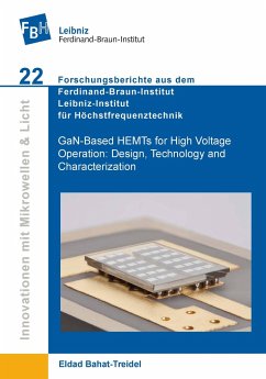
Gallium nitride (GaN)-based High Electron Mobility Transistors (HEMTs) for high voltage, high power switching and regulating for space applications are studied in this work. Efficient power switching is associated with operation in high OFF-state blocking voltage while keeping the ON-state resistance, the dynamic dispersion and leakage currents as low as possible. The potential of such devices to operate at high voltages is limited by a chain of factors such as subthreshold leakages and the device geometry. Blocking voltage enhancement is a complicated problem that requires parallel methods for solution; epitaxial layers design, device structural and geometry design, and suitable semiconductor manufacturing technique. In this work physical-based device simulation as an engineering tool was developed. An overview on GaN-based HEMTs physical based device simulation using Silvaco-¿ATLAS¿ is given. The simulation is utilized to analyze, give insight to the modes of operation of the device and for design and evaluation of innovative concepts. Physical-based models that describe the properties of the semiconductor material are introduced. A detailed description of the specific AlGaN/GaN HEMT structure definition and geometries are given along with the complex fine meshing requirements. Nitride-semiconductor specific material properties and their physical models are reviewed focusing on the energetic band structure, epitaxial strain tensor calculation in wurtzite materials and build-in polarization models. Special attention for thermal conductivity, carriers¿ mobility and Schottky-gate-reverse-bias-tunneling is paid. Empirical parameters matching and adjustment of models parameters to match the experimental device measured results are discussed.
Hinweis: Dieser Artikel kann nur an eine deutsche Lieferadresse ausgeliefert werden.
Hinweis: Dieser Artikel kann nur an eine deutsche Lieferadresse ausgeliefert werden.


