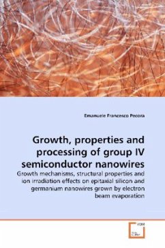
Nanowires are considered as a realistic addition in the future electronic and optoelectronic devices, as well as building blocks of the future photovoltaic cells and sensors. The recent progresses toward nanowire electronics are described and a brief selection of the very innovative and promising applications involving nanowires structures is shown. Thereafter, the main results about the control of the silicon and germanium nanowires features prepared by electron beam evaporation are discussed. It is possible to obtain single crystal, faceted nanowires epitaxially grown on top of the substrate and, by properly varying the experimental parameters, to determine the nanowires orientation, length and density. A microscopic model for the growth is proposed and the differences between Ge and Si nanowires are evidenced and discussed. After ion irradiation, nanowires bend and find a definitive structural modification by aligning themselves in the same direction of the beam. A complete recovery of the ion beam damage is obtained through thermal treatments, suggesting a complete recrystallization of their structure.
Bitte wählen Sie Ihr Anliegen aus.
Rechnungen
Retourenschein anfordern
Bestellstatus
Storno


