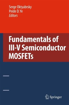
Issues relating to the high-K gate dielectric are among the greatest challenges for the evolving International Technology Roadmap for Semiconductors (ITRS). More than just an historical overview, this book will assess previous and present approaches related to scaling the gate dielectric and their impact, along with the creative directions and forthcoming challenges that will define the future of gate dielectric scaling technology. Topics include: an extensive review of Moore's Law, the classical regime for SiO2 gate dielectrics; the transition to silicon oxynitride gate dielectrics; the…mehr
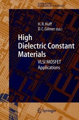
Issues relating to the high-K gate dielectric are among the greatest challenges for the evolving International Technology Roadmap for Semiconductors (ITRS). More than just an historical overview, this book will assess previous and present approaches related to scaling the gate dielectric and their impact, along with the creative directions and forthcoming challenges that will define the future of gate dielectric scaling technology. Topics include: an extensive review of Moore's Law, the classical regime for SiO2 gate dielectrics; the transition to silicon oxynitride gate dielectrics; the transition to high-K gate dielectrics (including the drive towards equivalent oxide thickness in the single-digit nanometer regime); and future directions and issues for ultimate technology generation scaling. The vision, wisdom, and experience of the team of authors will make this book a timely, relevant, and interesting, resource focusing on fundamentals of the 45 nm Technology Generation and beyond.
Classical Regime for SiO.- Brief Notes on the History of Gate Dielectrics in MOS Devices.- SiO2 Based MOSFETS: Film Growth and Si-SiO2 Interface Properties.- Oxide Reliability Issues.- The Economic Implications of Moore's Law.- Transition to Silicon Oxynitrides.- Gate Dielectric Scaling to 2.0-1.0 nm: SiO2 and Silicon Oxynitride.- Optimal Scaling Methodologies and Transistor Performance.- Silicon Oxynitride Gate Dielectric for Reducing Gate Leakage and Boron Penetration Prior to High-k Gate Dielectric Implementation.- Transition to High-k Gate Dielectrics.- Alternative Dielectrics for Silicon-Based Transistors: Selection Via Multiple Criteria.- Materials Issues for High-k Gate Dielectric Selection and Integration.- Designing Interface Composition and Structure in High Dielectric Constant Gate Stacks.- Electronic Structure of Alternative High-k Dielectrics.- Physicochemical Properties of Selected 4d, 5d, and Rare Earth Metals in Silicon.- High-k Gate Dielectric Deposition Technologies.- Issues in Metal Gate Electrode Selection for Bulk CMOS Devices.- CMOS IC Fabrication Issues for High-k Gate Dielectric and Alternate Electrode Materials.- Characterization and Metrology of Medium Dielectric Constant Gate Dielectric Films.- Electrical Measurement Issues for Alternative Gate Stack Systems.- High-k Gate Dielectric Materials Integrated Circuit Device Design Issues.- Future Directions for Ultimate Scaling Technology Generations.- High-k Crystalline Gate Dielectrics: A Research Perspective.- High-k Crystalline Gate Dielectrics: An IC Manufacturer's Perspective.- Advanced MOS-Devices.
Classical Regime for SiO.- Brief Notes on the History of Gate Dielectrics in MOS Devices.- SiO2 Based MOSFETS: Film Growth and Si—SiO2 Interface Properties.- Oxide Reliability Issues.- The Economic Implications of Moore's Law.- Transition to Silicon Oxynitrides.- Gate Dielectric Scaling to 2.0—1.0 nm: SiO2 and Silicon Oxynitride.- Optimal Scaling Methodologies and Transistor Performance.- Silicon Oxynitride Gate Dielectric for Reducing Gate Leakage and Boron Penetration Prior to High-k Gate Dielectric Implementation.- Transition to High-k Gate Dielectrics.- Alternative Dielectrics for Silicon-Based Transistors: Selection Via Multiple Criteria.- Materials Issues for High-k Gate Dielectric Selection and Integration.- Designing Interface Composition and Structure in High Dielectric Constant Gate Stacks.- Electronic Structure of Alternative High-k Dielectrics.- Physicochemical Properties of Selected 4d, 5d, and Rare Earth Metals in Silicon.- High-k Gate Dielectric Deposition Technologies.- Issues in Metal Gate Electrode Selection for Bulk CMOS Devices.- CMOS IC Fabrication Issues for High-k Gate Dielectric and Alternate Electrode Materials.- Characterization and Metrology of Medium Dielectric Constant Gate Dielectric Films.- Electrical Measurement Issues for Alternative Gate Stack Systems.- High-k Gate Dielectric Materials Integrated Circuit Device Design Issues.- Future Directions for Ultimate Scaling Technology Generations.- High-k Crystalline Gate Dielectrics: A Research Perspective.- High-k Crystalline Gate Dielectrics: An IC Manufacturer's Perspective.- Advanced MOS-Devices.
Es gelten unsere Allgemeinen Geschäftsbedingungen: www.buecher.de/agb
Impressum
www.buecher.de ist ein Internetauftritt der buecher.de internetstores GmbH
Geschäftsführung: Monica Sawhney | Roland Kölbl | Günter Hilger
Sitz der Gesellschaft: Batheyer Straße 115 - 117, 58099 Hagen
Postanschrift: Bürgermeister-Wegele-Str. 12, 86167 Augsburg
Amtsgericht Hagen HRB 13257
Steuernummer: 321/5800/1497