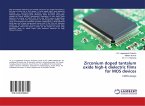
As CMOS integrated circuits are scaled down, conventional source/drain junction and contact technologies can no longer satisfy the requirements of MOSFETs, which require super-abrupt doping profiles and extremely low contact resistivities. To address these challenges, selective Si1-xGex source/drain technology can be a good candidate. In this approach, in-situ doped Si1-xGex layers are selectively deposited in recessed source/drain regions. Since the dopants occupy substitutional sites during epitaxial growth, high temperature annealing is not required for dopant activation, which eliminates diffusion and provides abrupt doping profiles. Furthermore, smaller bandgap of Si1-xGex reduces the metal-semiconductor barrier height, an essential requirement for achieving a substantial reduction in contact resistivity. Deposition selectivity of the process was studied and determined that high flows of PH3 could degrade the selectivity. An alternative deposition process based on alternating periods of deposition and etching was developed, which provided substantial improvements in deposition selectivity.
Bitte wählen Sie Ihr Anliegen aus.
Rechnungen
Retourenschein anfordern
Bestellstatus
Storno


