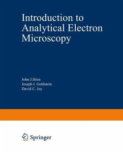
The birth of analytical electron microscopy (AEM) is somewhat obscure. Was it the recognition of the power and the development of STEM that signaled its birth? Was AEM born with the attachment of a crystal spectrometer to an otherwise conventional TEM? Or was it born earlier with the first analysis of electron loss spectra? It's not likely that any of these developments alone would have been sufficient and there have been many others (microdiffraction, EDS, microbeam fabrication, etc.) that could equally lay claim to being critical to the establishment of true AEM. It is probably more accurate to simply ascribe the present rapid development to the obvious: a combination of ideas whose time has come. Perhaps it is difficult to trace the birth of AEM simply because it remains a point of contention to even define its true scope. For example, the topics in this book, even though very broad, are still far from a complete description of what many call AEM. When electron beams interact with a solid it is well-known that a bewildering number of possible interactions follow. Analytical electron microscopy attempts to take full qualitative and quantitative advantage of as many of these interactions as possible while still preserving the capability of high resolution imaging. Although we restrict ourselves here to electron transparent films, much of what is described applies to thick specimens as well. Not surprisingly, signals from all possible interactions cannot yet (and probably never will) be attained simultaneously under optimum conditions.
Hinweis: Dieser Artikel kann nur an eine deutsche Lieferadresse ausgeliefert werden.
Hinweis: Dieser Artikel kann nur an eine deutsche Lieferadresse ausgeliefert werden.

