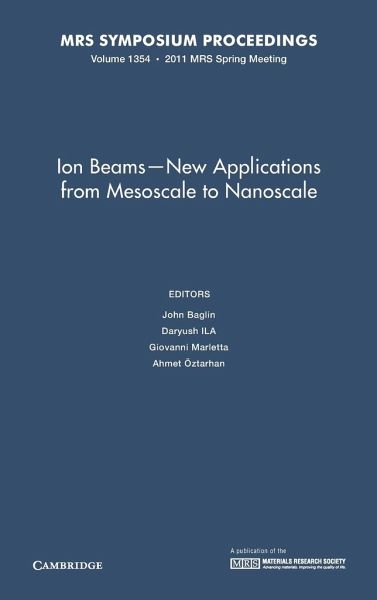
Ion Beams-New Applications from Mesoscale to Nanoscale
Herausgeber: Baglin, John; Marletta, Giovanni; Ila, Daryush
Ion Beams-New Applications from Mesoscale to Nanoscale
Herausgeber: Baglin, John; Marletta, Giovanni; Ila, Daryush
- Gebundenes Buch
- Merkliste
- Auf die Merkliste
- Bewerten Bewerten
- Teilen
- Produkt teilen
- Produkterinnerung
- Produkterinnerung
Symposium II, 'Ion Beams - New Applications from Mesoscale to Nanoscale', was held at the 2011 MRS Spring Meeting.
Andere Kunden interessierten sich auch für
- Ion Beams and Nano-Engineering41,99 €
- Ion Beams Nano-Engineering v1181148,99 €
- The Modifications of Metallic and Inorganic Materials by Using Energetic Ion/Electron Beams91,99 €
- Nanoscale Thermoelectric Materials88,99 €
- Micro-And Nanoscale Processing of Bomaterials40,99 €
- Probing Mechanics at Nanoscale Dimensions142,99 €
- Rudolf Gross / Anatolie Sidorenko / Lenar Tagirov (eds.)Nanoscale Devices - Fundamentals and Applications147,99 €
-
-
-
Symposium II, 'Ion Beams - New Applications from Mesoscale to Nanoscale', was held at the 2011 MRS Spring Meeting.
Hinweis: Dieser Artikel kann nur an eine deutsche Lieferadresse ausgeliefert werden.
Produktdetails
- Produktdetails
- Verlag: Cambridge University Press
- Seitenzahl: 176
- Erscheinungstermin: 23. Februar 2012
- Englisch
- Abmessung: 235mm x 157mm x 14mm
- Gewicht: 415g
- ISBN-13: 9781605113319
- ISBN-10: 160511331X
- Artikelnr.: 34674542
- Herstellerkennzeichnung
- Produktsicherheitsverantwortliche/r
- Europaallee 1
- 36244 Bad Hersfeld
- gpsr@libri.de
Part I. Reviews and Research Reports: 1. Universal biomolecule binding
interlayers created by energetic ion bombardment Marcela Bilek; 2. Neural
cell attachment on metal ion implanted glass surfaces Emel Sokullu Urkac;
3. Cluster ion beam processing: review of current and prospective
applications Isao Yamada; 4. Nano-engineering with a focused helium ion
beam Diederik Maas; 5. Multi-ion beam lithography and processing studies
Bill Appleton; 6. Ion irradiation effects in silicon nanowires Kai
Nordlund; 7. Folding graphene with swift heavy ions Sevilay Akcöltekin; 8.
Ion irradiation on phase change materials Emanuele Rimini; 9. Ion beams for
synthesis and modifications of nanostructures in semiconductors Anand
Pathak; 10. Raman scattering study of Si nanoclusters formed in Si through
a double Au implantation Durga Mahapatra; 11. Effects of hydrogen ion
implantation and thermal annealing on structural and optical properties of
single-crystal sapphire Mengbing Huang; 12. Post-CMOS integration of
nanomechanical devices by direct ion beam irradiation of silicon Francesc
Perez-Murano; 13. Enhanced adhesion of coating layers by ion beam mixing:
an application for nuclear hydrogen production Jae-Won Park; 14. Structural
changes induced by swift heavy ion beams in tensile strained
Al(1-x)InxN/GaN hetero-structures Anand Pathak; 15. 5 MeV Si ion
modification on thermoelectric SiO2/SiO2+Cu multilayer films Cydale Smith;
16. Study of scalable IBS nanopatterning mechanisms for III-V
semiconductors using in-situ surface characterization Jean-Paul Allain; 17.
Modeling of approximated electron transport across ion beam patterned
quantum dot nanostructures Jonathan Lassiter; 18. RBS, XRD, raman and AFM
studies of microwave synthesized Ge nanocrystals Anand Pathak; 19.
Comparison of ion beam and electron beam induced transport of hot charge
carriers in metal-insulator-metal junctions Marika Schleberger; Part II.
Forum Report: 20. Future directions for ion beam technology and research:
forum report John Baglin.