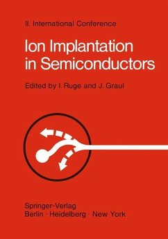
Ion Implantation in Semiconductors
Proceedings of the II. International Conference on Ion Implantation in Semiconductors, Physics and Technology, Fundamental and Applied Aspects May 24¿28, 1971, Garmisch-Partenkirchen, Bavaria, Germany
Herausgegeben von Ruge, Ingolf; Graul, J.
Ion Implantation in Semiconductors
Proceedings of the II. International Conference on Ion Implantation in Semiconductors, Physics and Technology, Fundamental and Applied Aspects May 24¿28, 1971, Garmisch-Partenkirchen, Bavaria, Germany
Herausgegeben von Ruge, Ingolf; Graul, J.
- Broschiertes Buch
- Merkliste
- Auf die Merkliste
- Bewerten Bewerten
- Teilen
- Produkt teilen
- Produkterinnerung
- Produkterinnerung
In recent years great progress has been made in the field of ion implantation, particularly with respect to applications in semiconductors. It would be impos sible not to note the growing interest in this field, both by research groups and those directly concerned with production of devices. Furthermore, as several papers have pointed out, ion implantation and its associated technologies promise exciting advances in the development of new kinds of devices and provide power ful new tools for materials investigations. It was, therefore, appropriate to arrange the II. International Conference on…mehr
Andere Kunden interessierten sich auch für
![Fremdkörpersarkome Fremdkörpersarkome]() G. OttFremdkörpersarkome39,99 €
G. OttFremdkörpersarkome39,99 €![Anaesthesie im Alter Anaesthesie im Alter]() Anaesthesie im Alter54,99 €
Anaesthesie im Alter54,99 €![Theorie und Praxis der Steinachschen Operation Theorie und Praxis der Steinachschen Operation]() Peter SchmidtTheorie und Praxis der Steinachschen Operation54,99 €
Peter SchmidtTheorie und Praxis der Steinachschen Operation54,99 €![Green and Sustainable Pharmacy Green and Sustainable Pharmacy]() Green and Sustainable Pharmacy116,99 €
Green and Sustainable Pharmacy116,99 €![Détermination des paramètres d'acquisition du scanner Détermination des paramètres d'acquisition du scanner]() Yasmin SoleymanDétermination des paramètres d'acquisition du scanner21,99 €
Yasmin SoleymanDétermination des paramètres d'acquisition du scanner21,99 €![Determination of the CT scan parameters Determination of the CT scan parameters]() Yasmin SoleymanDetermination of the CT scan parameters21,99 €
Yasmin SoleymanDetermination of the CT scan parameters21,99 €![Chirurgisches Forum '77 für experimentelle und klinische Forschung Chirurgisches Forum '77 für experimentelle und klinische Forschung]() Chirurgisches Forum '77 für experimentelle und klinische Forschung54,99 €
Chirurgisches Forum '77 für experimentelle und klinische Forschung54,99 €-
-
-
In recent years great progress has been made in the field of ion implantation, particularly with respect to applications in semiconductors. It would be impos sible not to note the growing interest in this field, both by research groups and those directly concerned with production of devices. Furthermore, as several papers have pointed out, ion implantation and its associated technologies promise exciting advances in the development of new kinds of devices and provide power ful new tools for materials investigations. It was, therefore, appropriate to arrange the II. International Conference on Ion Implantation in Semiconductors within the rather short time of one year since the first conference was held in 1970 in Thousand Oaks, California. Although ori ginally planned on a small scale with a very limited number of participants, more than two hundred scientists from 15 countries participated in the Conference which was held May 24 - 28, 1971 at the Congress Center in Garmisch-Partenkirchen. This volume contains the papers that were presented at the Conference. Due to the tremendous volume of research presented, publication here of all the works in full detail was not possible. Many authors therefore graciously agreed to submit abbreviated versions of their papers.
Hinweis: Dieser Artikel kann nur an eine deutsche Lieferadresse ausgeliefert werden.
Hinweis: Dieser Artikel kann nur an eine deutsche Lieferadresse ausgeliefert werden.
Produktdetails
- Produktdetails
- Verlag: Springer / Springer Berlin Heidelberg / Springer, Berlin
- Artikelnr. des Verlages: 978-3-642-80662-9
- Softcover reprint of the original 1st ed. 1971
- Seitenzahl: 532
- Erscheinungstermin: 25. Dezember 2011
- Englisch
- Abmessung: 244mm x 170mm x 29mm
- Gewicht: 907g
- ISBN-13: 9783642806629
- ISBN-10: 3642806627
- Artikelnr.: 36114619
- Herstellerkennzeichnung Die Herstellerinformationen sind derzeit nicht verfügbar.
I. Disorder in Ion Implanted Silicon.- 1.1 Ionization and Thermal Dependences of Implantation Disorder in Silicon.- 1.2 Localized Mode of Substitutional Carbon in Ion-Implanted Silicon.- 1.3 Inventory of Paramagnetic Defects in Ion-Implanted Silicon.- 1.4 Structural Differences in Light and Heavy Ion Disorder in Si Studied by Single and Double Alignment Channeling Techniques.- 1.5 Investigation of Ion Implantation Damage with Stress Measurements.- 1.6 Energy Levels of Defects in Ion Implanted Silicon.- 1.7 Photoconductivity of Boron Implanted Silicon.- 1.8 Electron Paramagnetic Resonance on Divacancies in Phosphorus-Implanted Silicon.- II. Implantation of Boron and Phosphorus into Silicon.- II. 1 Distribution of Boron Implanted Silicon.- 11.2 Phosphorus Channeled in Silicon: Profiles and Electrical Activity.- 11.3 Enhanced Annealing Effects of Boron Implanted Layers in Silicon by Post-Implantation of Silicon Ions.- 11.4 Electrical Profiles of Ion Implanted Silicon and their Comparison with Defect Structures.- 11.5 A New Method for Boron Doping of Silicon by Implantation of BF2-Molecules.- 11.6 Crystal Defects and Electrical Properties in Ion-Implanted Silicon.- 11.7 Amorphization of Silicon Crystals Bombarded by 30 keV Phosphorus Ions at Different Temperatures.- 11.8 Additional Ion Bombardment of Well Annealed Silicon Crystals Implanted with Phosphorus and Arsenic.- 11.9 The Influence of Ion Beam Current Densities on the Electrical Properties of Boron Implanted Silicon.- II. 10 The Evaluation of Electrically Active Damage in Hot, Phosphorus Implantations in Silicon by Means of Hall-Effect Measurements.- III. Implantation into Compound Semiconductors.- III. 1 Backscattering Analysis and Electrical Behavior of SiC Implanted with 40 keV Indium.- III.2 Anomalous Diffusion of Defects in Ion-Implanted GaAs.- III. 3 Enhanced Diffusion in Ion-Bombarded GaAs.- III.4 The Effects of Dose Rate and Implantation Temperature on Lattice Damage and Electrical Activity in Ion Implanted GaAs.- III.5 The Effects of Arsenic Ion Implantation in GaAs.- III. 6 Implantation of Zinc into GaAs at 1 MeV.- III.7 Implantation of Bi into GaP III. Hot-Implant Behaviour.- III.8 The Influence of Various Parameters on Radiation Damage in GaP.- III.9 The Retention of Bi Ions Implanted in GaAs.- III.10 The Annealing Behaviour of Gallium Phosphide in the Region 110-500°K after 300 keV Neon Irradiation.- IV. Compound and Amorphous Semiconductors.- IV. 1 Compensation of N-Type GaAs by Proton Bombardement.- IV.2 Ion Implanted p-n Junctions in GaAs0.6P0.4.- IV. 3 Lattice Disorder and Outdiffusion in Ion Implanted InSb and CdTe.- IV.4 Ion-Implantation of Nitrogen into n-Type Cadmium Sulfide.- IV.5 Infrared Studies of SiC, Si3N4, and SiO2 Formation in Ion-Implanted Silicon.- IV. 6 Ion Implantation and Amorphous Materials.- IV.7 Raman Spectra of Amorphous Semiconductors Prepared by Ion Bombardement.- IV.8 Effects of Implantation on Thin Layers of Aluminum Metallization on Silicon.- IV. 9 Crystalline to Amorphous Transformation in Ion-Bombarded Silicon.- V. Techniques and Germanium.- V. 1 Analysis of Contact Formation and Surface Layers on Semiconductors.- V. 2 New Aspects of Atom Location: Flux Peaking.- V.3 Dimpling - a New Manifestation of Ion Produced Lattice Damage.- V.4 The Use of Ion-Induced X-Rays to Investigate the Concentration Distribution and Atom Location of Boron-Implanted Silicon.- V. 5 Electrical Properties of Ion Implanted Germanium.- VI. Devices 1.- VI. 1 Recent Advances in Ion Implanted MOS Technology.- VI.2 Recent Advances in Ion Implanted Junction-DeviceTechnology.- VI. 3 Enhanced Diffusion of Substrate Impurities into Epitaxial Layers in Si by Proton Irradiation.- VI.4 Junction Field Effect Transistors Fabricated by Ion Implantation.- VI. 5 Microwave Transistors Fabricated by I on-Implantation Selection of Doping Impurities and Phototype Realization.- VI.6 Application of Ion Implantation to N-P-N-Transistors.- VI.7 New Techniques for Improving High Value Ion Implanted Resistors.- VI.8 Piezoresistive Properties of Ion Implanted Layers in Silicon.- VII. Devices 2.- VII.1 Surface States Induced by Ion Implantation.- VII.2 Speed Improvement of Ion Implanted Self Aligned Gate MOS Transistors.- VII. 3 Chemical and Electrical Behaviour of Ion Implanted SiO2 Films.- VII.4 Ion Implanted Thermoresistive Device for Cryogenic Temperatures.- VII.5 Ion Implanted Light Sensing Diodes.- VII.6 The Application of Ion Implantation to Avalanche Multiplication Devices.- VII.7 Ion Implanted p-n Junctions in Near Intrinsic n-Type Silicon for Nuclear Particle Detectors.- VII.8 Boron Implanted Contacts on High Purity Germanium.- VII.9 New Ion Implantation Areas.- VIII. Implantation into Silicon.- VIII. 1 Non-Gaussian Implantation Profiles.- VIII. 2 Atom Location in the Case of Enhanced Diffusion Measured by Backscattering Method.- VIII.3 Enhanced Diffusion and Electrical Properties of Ion Implanted Silicon.- VIII.4 The Presence of Deep Levels in Silicon Implanted with Channeled Low Energy Phosphorus Ions.- VIII.5 Mobility, Resistivity and Carrier Concentration Measured on Silicon Implanted with Channeled and Nonchanneled Indium Ions.- VIII.6 Ionization Energy Determination in Indium Implanted Silicon.- VIII.7 Some Observations on High Energy Nitrogen Implantations in Silicon.- VIII.8 Nitrogen Implantation of p-Silicon at Cryogenic Temperatures.- VIII.9 Conductive Properties of the Ion Implanted Binary System Si1-XA1X.
I. Disorder in Ion Implanted Silicon.- 1.1 Ionization and Thermal Dependences of Implantation Disorder in Silicon.- 1.2 Localized Mode of Substitutional Carbon in Ion-Implanted Silicon.- 1.3 Inventory of Paramagnetic Defects in Ion-Implanted Silicon.- 1.4 Structural Differences in Light and Heavy Ion Disorder in Si Studied by Single and Double Alignment Channeling Techniques.- 1.5 Investigation of Ion Implantation Damage with Stress Measurements.- 1.6 Energy Levels of Defects in Ion Implanted Silicon.- 1.7 Photoconductivity of Boron Implanted Silicon.- 1.8 Electron Paramagnetic Resonance on Divacancies in Phosphorus-Implanted Silicon.- II. Implantation of Boron and Phosphorus into Silicon.- II. 1 Distribution of Boron Implanted Silicon.- 11.2 Phosphorus Channeled in Silicon: Profiles and Electrical Activity.- 11.3 Enhanced Annealing Effects of Boron Implanted Layers in Silicon by Post-Implantation of Silicon Ions.- 11.4 Electrical Profiles of Ion Implanted Silicon and their Comparison with Defect Structures.- 11.5 A New Method for Boron Doping of Silicon by Implantation of BF2-Molecules.- 11.6 Crystal Defects and Electrical Properties in Ion-Implanted Silicon.- 11.7 Amorphization of Silicon Crystals Bombarded by 30 keV Phosphorus Ions at Different Temperatures.- 11.8 Additional Ion Bombardment of Well Annealed Silicon Crystals Implanted with Phosphorus and Arsenic.- 11.9 The Influence of Ion Beam Current Densities on the Electrical Properties of Boron Implanted Silicon.- II. 10 The Evaluation of Electrically Active Damage in Hot, Phosphorus Implantations in Silicon by Means of Hall-Effect Measurements.- III. Implantation into Compound Semiconductors.- III. 1 Backscattering Analysis and Electrical Behavior of SiC Implanted with 40 keV Indium.- III.2 Anomalous Diffusion of Defects in Ion-Implanted GaAs.- III. 3 Enhanced Diffusion in Ion-Bombarded GaAs.- III.4 The Effects of Dose Rate and Implantation Temperature on Lattice Damage and Electrical Activity in Ion Implanted GaAs.- III.5 The Effects of Arsenic Ion Implantation in GaAs.- III. 6 Implantation of Zinc into GaAs at 1 MeV.- III.7 Implantation of Bi into GaP III. Hot-Implant Behaviour.- III.8 The Influence of Various Parameters on Radiation Damage in GaP.- III.9 The Retention of Bi Ions Implanted in GaAs.- III.10 The Annealing Behaviour of Gallium Phosphide in the Region 110-500°K after 300 keV Neon Irradiation.- IV. Compound and Amorphous Semiconductors.- IV. 1 Compensation of N-Type GaAs by Proton Bombardement.- IV.2 Ion Implanted p-n Junctions in GaAs0.6P0.4.- IV. 3 Lattice Disorder and Outdiffusion in Ion Implanted InSb and CdTe.- IV.4 Ion-Implantation of Nitrogen into n-Type Cadmium Sulfide.- IV.5 Infrared Studies of SiC, Si3N4, and SiO2 Formation in Ion-Implanted Silicon.- IV. 6 Ion Implantation and Amorphous Materials.- IV.7 Raman Spectra of Amorphous Semiconductors Prepared by Ion Bombardement.- IV.8 Effects of Implantation on Thin Layers of Aluminum Metallization on Silicon.- IV. 9 Crystalline to Amorphous Transformation in Ion-Bombarded Silicon.- V. Techniques and Germanium.- V. 1 Analysis of Contact Formation and Surface Layers on Semiconductors.- V. 2 New Aspects of Atom Location: Flux Peaking.- V.3 Dimpling - a New Manifestation of Ion Produced Lattice Damage.- V.4 The Use of Ion-Induced X-Rays to Investigate the Concentration Distribution and Atom Location of Boron-Implanted Silicon.- V. 5 Electrical Properties of Ion Implanted Germanium.- VI. Devices 1.- VI. 1 Recent Advances in Ion Implanted MOS Technology.- VI.2 Recent Advances in Ion Implanted Junction-DeviceTechnology.- VI. 3 Enhanced Diffusion of Substrate Impurities into Epitaxial Layers in Si by Proton Irradiation.- VI.4 Junction Field Effect Transistors Fabricated by Ion Implantation.- VI. 5 Microwave Transistors Fabricated by I on-Implantation Selection of Doping Impurities and Phototype Realization.- VI.6 Application of Ion Implantation to N-P-N-Transistors.- VI.7 New Techniques for Improving High Value Ion Implanted Resistors.- VI.8 Piezoresistive Properties of Ion Implanted Layers in Silicon.- VII. Devices 2.- VII.1 Surface States Induced by Ion Implantation.- VII.2 Speed Improvement of Ion Implanted Self Aligned Gate MOS Transistors.- VII. 3 Chemical and Electrical Behaviour of Ion Implanted SiO2 Films.- VII.4 Ion Implanted Thermoresistive Device for Cryogenic Temperatures.- VII.5 Ion Implanted Light Sensing Diodes.- VII.6 The Application of Ion Implantation to Avalanche Multiplication Devices.- VII.7 Ion Implanted p-n Junctions in Near Intrinsic n-Type Silicon for Nuclear Particle Detectors.- VII.8 Boron Implanted Contacts on High Purity Germanium.- VII.9 New Ion Implantation Areas.- VIII. Implantation into Silicon.- VIII. 1 Non-Gaussian Implantation Profiles.- VIII. 2 Atom Location in the Case of Enhanced Diffusion Measured by Backscattering Method.- VIII.3 Enhanced Diffusion and Electrical Properties of Ion Implanted Silicon.- VIII.4 The Presence of Deep Levels in Silicon Implanted with Channeled Low Energy Phosphorus Ions.- VIII.5 Mobility, Resistivity and Carrier Concentration Measured on Silicon Implanted with Channeled and Nonchanneled Indium Ions.- VIII.6 Ionization Energy Determination in Indium Implanted Silicon.- VIII.7 Some Observations on High Energy Nitrogen Implantations in Silicon.- VIII.8 Nitrogen Implantation of p-Silicon at Cryogenic Temperatures.- VIII.9 Conductive Properties of the Ion Implanted Binary System Si1-XA1X.

