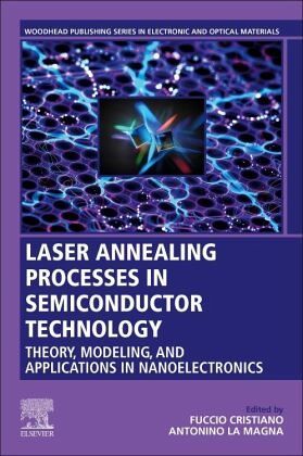
Laser Annealing Processes in Semiconductor Technology
Theory, Modeling and Applications in Nanoelectronics
Herausgegeben: Cristiano, Fuccio; La Magna, Antonino

PAYBACK Punkte
82 °P sammeln!
Laser Annealing Processes in Semiconductor Technology: Theory, Modeling and Applications in Nanoelectronics synthesizes the scientific and technological advances of laser annealing processes for current and emerging nanotechnologies. The book provides an overview of the laser-matter interactions of materials and recent advances in modeling of laser-related phenomena, with the bulk of the book focusing on current and emerging (beyond-CMOS) applications. Reviewed applications include laser annealing of CMOS, group IV semiconductors, superconducting materials, photonic materials, 2D materials. Th...
Laser Annealing Processes in Semiconductor Technology: Theory, Modeling and Applications in Nanoelectronics synthesizes the scientific and technological advances of laser annealing processes for current and emerging nanotechnologies. The book provides an overview of the laser-matter interactions of materials and recent advances in modeling of laser-related phenomena, with the bulk of the book focusing on current and emerging (beyond-CMOS) applications. Reviewed applications include laser annealing of CMOS, group IV semiconductors, superconducting materials, photonic materials, 2D materials. This comprehensive book is ideal for post-graduate students, new entrants, and experienced researchers in academia, research and development in materials science, physics and engineering.


