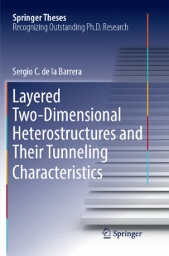
This thesis demonstrates that layered heterostructures of two-dimensional crystals graphene, hexagonal boron nitride, and transition metal dichalcogenides provide new and interesting interlayer transport phenomena. Low-energy electron microscopy is employed to study the surface of atomically thin WSe2 prepared by metal-organic chemical vapor deposition on epitaxial graphene substrates, and a method for unambiguously measuring the number of atomic layers is presented. Using very low-energy electrons to probe the surface of similar heterostructures, a relationship between extracted work function differences from the layers and the nature of the electrical contact between them is revealed. An extension of this analysis is applied to surface studies of MoSe2 prepared by molecular beam epitaxy on epitaxial graphene. A large work function difference is measured between the MoSe2 and graphene, and a model is provided which suggests that this observation results from an exceptional defect density in the MoSe2 film. The thesis expounds a theory for computing tunneling currents between two-dimensional crystals separated by a thin insulating barrier; a few situations resulting in resonant tunneling and negative differential resistance are illustrated by computed examples, as well as observed characteristics, for monolayer and bilayer graphene tunneling junctions and transistors.
Bitte wählen Sie Ihr Anliegen aus.
Rechnungen
Retourenschein anfordern
Bestellstatus
Storno

