Localization Effects in Disordered III-V Semiconductor Nanostructures
-
- Taschenbuch ausgewählt
- eBook
-
Sprache:Englisch
22,99 €
inkl. gesetzl. MwSt.,
Beschreibung
Produktdetails
Einband
Taschenbuch
Erscheinungsdatum
07.12.2015
Verlag
Cuvillier VerlagSeitenzahl
120
Maße (L/B/H)
21/14,8/0,7 cm
Gewicht
167 g
Sprache
Englisch
ISBN
978-3-7369-9160-6
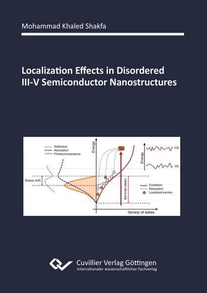
Due to the increasing demands industrially as well as scientifically on new optoelectronic devices for specific applications, semiconductor materials with desired energy band-gap are needed. In this context, alloying provides the ability to tailor the energy band gap of a compound semiconductor (ternary or quaternary) through the manipulation of its constituent composition. In this thesis, It is focused on two different III-V-based compound semiconductor materials, Ga(NAsP) and Ga(AsBi), both are promising for long-wavelength optoelectronic applications. In particular, quaternary Ga(NAsP) semiconductor structures can be utilized for the fabrication of intermediate band solar cells, for infrared laser emission, and, with a tremendous potential, for the realization of monolithic optoelectronic integrated circuits on silicon substrate (silicon photonics). On the other hand, ternary Ga(AsBi) semiconductor structures have been employed for a variety of applications including, for example, but not limited to, photoconductive terahertz antennas, light-emitting diodes (LEDs), and optically pumped as well as electrically injected laser diodes. Band gap engineering is achieved in the studied GaAs-based compounds by varying the amount of the incorporated V-element, i.e., nitrogen or bismuth. Despite the advantage of a shrinking in the band-gap energy, the introduction of a small amount of a V-element to a GaAs host structure results in an increase in the disorder potential due to the differences, e.g., in size and electronegativity between the incorporated and substituted anions. The presence of disorder effects within a semiconductor can significantly influence its electronic structure, i.e., the density of localized states (DOS) is increased. Disorder-induced localized states drastically affect carrier recombination processes in semiconductors. The changes in carrier dynamics can be revealed by investigating, e.g., electrical and optical properties of disordered semiconductors. In the presented work, photoluminescence (PL) spectroscopy measurements are employed for the characterization of disorder in semiconductor nanostructures. Beside the need of a qualitative explanation, a quantitative description of disorder effects, i.e., energy scaling of the disorder potential, is a task of crucial importance. Both aspects are discussed through the thesis.
Noch keine Bewertungen vorhanden
Verfassen Sie die erste Bewertung zu diesem Artikel
Helfen Sie anderen Kundinnen und Kunden durch Ihre Meinung.
Kurze Frage zu unserer Seite
Vielen Dank für dein Feedback
Wir nutzen dein Feedback, um unsere Produktseiten zu verbessern. Bitte habe Verständnis, dass wir dir keine Rückmeldung geben können. Falls du Kontakt mit uns aufnehmen möchtest, kannst du dich aber gerne an unseren Kund*innenservice wenden.
zum Kundenservice