
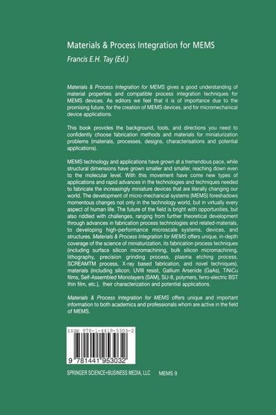
• Produktbild: Materials & Process Integration for MEMS
  • Produktbild: Materials & Process Integration for MEMS
Band 9 - 13%

Materials & Process Integration for MEMS

Aus der Reihe Microsystems
13% sparen

138,99 € UVP 160,49 €

inkl. gesetzl. MwSt., Versandkostenfrei


Beschreibung

Produktdetails

Einband

Taschenbuch

Erscheinungsdatum

03.12.2010

Abbildungen

XIX, 299 p.

Herausgeber

Francis E. H. Tay

Verlag

Springer Us

Seitenzahl

299

Maße (L/B/H)

23,5/15,5/1,8 cm

Gewicht

499 g

Auflage

Softcover reprint of hardcover 1st edition 2002

Sprache

Englisch

ISBN

978-1-4419-5303-2

Beschreibung

Produktdetails

Einband

Taschenbuch

Erscheinungsdatum

03.12.2010

Abbildungen

XIX, 299 p.

Herausgeber

Francis E. H. Tay

Verlag

Springer Us

Seitenzahl

299

Maße (L/B/H)

23,5/15,5/1,8 cm

Gewicht

499 g

Auflage

Softcover reprint of hardcover 1st edition 2002

Sprache

Englisch

ISBN

978-1-4419-5303-2

Herstelleradresse

Springer-Verlag GmbH
Tiergartenstr. 17
69121 Heidelberg
DE

Email: ProductSafety@springernature.com

Noch keine Bewertungen vorhanden

Verfassen Sie die erste Bewertung zu diesem Artikel

Helfen Sie anderen Kundinnen und Kunden durch Ihre Meinung.

Kundinnen und Kunden meinen

Bewertungen (0)

  • Produktbild: Materials & Process Integration for MEMS
  • Produktbild: Materials & Process Integration for MEMS
  • 1. Integration of Piezoelectric Pb (ZrxTi1?x)03 (PZT) Thin Films into Micromachined Sensors and Actuators.- 2. Porous Silicon as a Sacrificial Layer in Production of Silicon Diaphragms by Precision Grinding.- 3. GaAs Cantilever and Bridge Membrane-Like Structures Fully Compatible with AlGaAs/InGaAs/GaAs and InGaP/InGaAs/GaAs Based HFETs.- 4. Magnetron Sputtered TiNiCu Shape Memory Alloy Thin Film for MEMS Applications.- 5. Chemically Amplified Resist for Micromachining using X-Ray Lithography.- 6. Self-Assembled Monolayers (SAM) for Tunneling Sensors.- 7. Oxidation Process-Optimization for Large Area Silicon Fusion Bonded Devices and MEMS Structures.- 8. Silicon Nanomachining by Scanning Probe Lithography and Anisotropie Wet Etching.- 9. A Novel Bulk Micromachining Method in Gallium Arsenide.- 10. Deep X-Ray Lithography for MEMS-Photoelectron Exposure of the Upper and Bottom Resist Layers.- 11. Spray Coating Technology of Photoresist/Polymer for 3-D Patterning and Interconnect.- 12. Uncooled Infrared Image Sensor of Dielectric Bolometer Mode using Ferroelectric BST Thin Film Prepared by Metal Organic Decomposition.- 13. Tactical Grade MEMS Gyroscopes Fabricated by the SBM Process.- 14. Plasma Etching Techniques to Form High-Aspect-Ratio MEMS Structures.