The fast-developing information technology industry is driving a need for new materials in order to facilitate the development of more reliable microelectronic products. Materials for Information Technology is an up-to-date overview of current developments and R&D activities in the field of materials used for information technology with a focus on future applications. Included are: materials for silicon-based semiconductor devices (including high-k gate dielectric materials); materials for nonvolatile memories; materials for on-chip interconnects and interlayer dielectrics…mehr
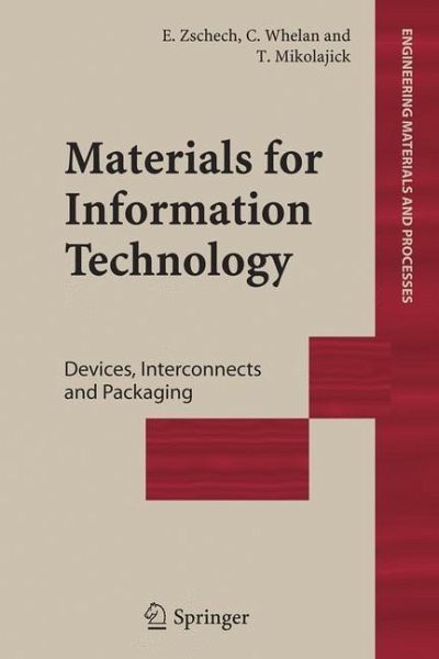
The fast-developing information technology industry is driving a need for new materials in order to facilitate the development of more reliable microelectronic products.
Materials for Information Technology is an up-to-date overview of current developments and R&D activities in the field of materials used for information technology with a focus on future applications. Included are:
materials for silicon-based semiconductor devices (including high-k gate dielectric materials);
materials for nonvolatile memories;
materials for on-chip interconnects and interlayer dielectrics (including silicides, barrier materials, low-k and ultra low-k dielectric materials); and
materials for assembly and packaging
The latest results in materials science and engineering as well as applications in the semiconductor industry are covered including the synthesis of blanket and patterned thin film materials, their properties, constitution, structure and microstructure. Computer modelling and analytical techniques to characterise thin film structures are also included to give a comprehensive survey of materials for the IT industry.
The Engineering Materials and Processes series focuses on all forms of materials and the processes used to synthesise and formulate them as they relate to the various engineering disciplines. The series deals with a diverse range of materials: ceramics; metals (ferrous and non-ferrous); semiconductors; composites, polymers, biomimetics etc. Each monograph in the series is written by a specialist and demonstrates how enhancements in materials and the processes associated with them can improve performance in the field of engineering in which they are used.
Dr Ehrenfried Zschech is manager of the Materials Analysis Department at AMD Saxony LLC & Co. KG in Dresden, Germany. Advanced Microdevices (AMD) is a global manufacturer of microprocessors and other integrated circuit-based products. AMD's manufacturing facility in Dresden is the company's most advanced and the site also hosts the company's European R&D centre. Dr Zschech was the coordinator of the IT topic of EUROMAT 2003 in Lausanne. This book, although not a proceedings, has resulted from his work for the conference. It collects contributions on materials for information technology applications from the author's of conference papers as well as chapters from other authors in order to create a state-of-the art edited volume on the subject from the world's leading experts in academia and industry. Dr Caroline Whelan is a researcher at the Interuniversity MicroElectronics Center (IMEC) Leuven, Belgium, a leading research institution in microelectronics funded by industry, government, ESA and the EU. Dr Thomas Mikolajick is a researcher at Infineon Technologies AG, a German-based IC products manufacturers. Infineon's R&D activities cover innovations in nano technologies, photonics, high frequency circuits, mixed signal circuits, electronic biosensors, systems technology, emerging applications.
Inhaltsangabe
Recent Advances in Thin-film Deposition.- Molecular-beam Deposition of High-k Gate Dielectrics for Advanced CMOS.- LEPECVD - A Production Technique for SiGe MOSFETs and MODFETs.- Thin-film Engineering by Atomic-layer Deposition for Ultra-scaled and Novel Devices.- Atomic-layer Deposited Barrier and Seed Layers for Interconnects.- Copper CVD for Conformal Ultrathin-film Deposition.- Pushing PVD to the Limits - Recent Advances.- Surface Engineering Using Self-assembled Monolayers: Model Substrates for Atomic-layer Deposition.- Selective Airgaps: Towards a Scalable Low-k Solution.- Silicides - Recent Advances and Prospects.- TEM Characterization of Strained Silicon.- Material Aspects of Non-Volatile Memories.- An Introduction to Nonvolatile Memory Technology.- Floating-dot Memory Transistors on SOI Substrate.- Ion-beam Synthesis of Nanocrystals for Multidot Memory Structures.- Scaling of Ferroelectric-based Memory Concepts.- Device Concepts with Magnetic Tunnel Junctions.- Phase-change Memories.- Amorphous-to-fcc Transition in GeSbTe Alloys.- Organic Nonvolatile Memories.- Materials for Interconnects.- Interconnect Technology - Today, Recent Advances and a Look into the Future.- Dielectric and Scaling Effects on Electromigration for Cu Interconnects.- Texture and Stress Study of Sub-Micron Copper Interconnect Lines Using X-ray Microdiffraction.- Stress Modeling for Copper Interconnect Structures.- Conductivity Enhancement in Metallization Structures of Regular Grains.- Advanced Barriers for Copper Interconnects.- Synthesis and Characterization of Compounds Obtained by Crosslinking of Polymethylhydrosiloxane by Aromatic Rings.- Revealing the Porous Structure of Low-k Materials Through Solvent Diffusion.- Carbon Nanotube Via Technologies for Future LSIInterconnects.- Nickel Nanowires Obtained by Template Synthesis.- Materials for Assembly/Packaging.- The Importance of Polymers in Wafer-Level Packaging.- Electrically Conductive Adhesives as Solder Alternative: A Feasible Challenge.- The Role of Au/Sn Solder in Packaging.- Packaging Materials: Organic-Inorganic Hybrids for Millimetre-Wave Optoelectronics.- Wafer-Level Three-Dimensional Hyper-Integration Technology Using Dielectric Adhesive Wafer Bonding.- Advanced Materials Characterization.- Challenges to Advanced Materials Characterization for ULSI Applications.- Advanced Material Characterization by TOFSIMS in Microelectronic.- Electronic Properties of the Interface Formed by Pr2O3 Growth on Si(001), Si(111) and SiC(0001) Surfaces.- Materials Characterization by Ellipsometry.- Thermal Desorption Spectrometry as a Method of Analysis for Advanced Interconnect Materials.- Electron Backscatter Diffraction: Application to Cu Interconnects in Top-View and Cross Section.- X-ray Reflectivity Characterisation of Thin-Film and Multilayer Structures.
Es gelten unsere Allgemeinen Geschäftsbedingungen: www.buecher.de/agb
Impressum
www.buecher.de ist ein Internetauftritt der buecher.de internetstores GmbH
Geschäftsführung: Monica Sawhney | Roland Kölbl | Günter Hilger
Sitz der Gesellschaft: Batheyer Straße 115 - 117, 58099 Hagen
Postanschrift: Bürgermeister-Wegele-Str. 12, 86167 Augsburg
Amtsgericht Hagen HRB 13257
Steuernummer: 321/5800/1497