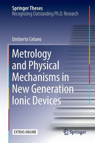
This thesis presents the first direct observations of the 3D-shape, size and electrical properties of nanoscale filaments, made possible by a new Scanning Probe Microscopy-based tomography technique referred to as scalpel SPM. Using this innovative technology and nm-scale observations, the author achieves essential insights into the filament formation mechanisms, improves the understanding required for device optimization, and experimentally observes phenomena that had previously been only theoretically proposed.
Umberto Celano received a M.Sc. degree in Nanoelectronics from the University of Rome ``Sapienza'', Italy and a Ph.D. degree in Physics from the KU Leuven, Belgium in 2011 and 2015 respectively. Currently, he is a researcher in the material and component analysis group of imec in Belgium. Umberto's research interests include nanometer scale issues in materials, emerging nanoelectronics and physical characterization. His goal is to explore methods and novel metrology techniques that enable the understanding of the physics in nanomaterials and nanoelectronics devices.
Inhaltsangabe
Introduction.- Filamentary-Based Resistive Switching.- Nanoscaled Electrical Characterization.- Conductive Filaments: Formation, Observation and Manipulation.- Three-Dimensional Filament Observation.- Reliability Threats in CBRAM.- Conclusions and Outlook.