- Gebundenes Buch
- Merkliste
- Auf die Merkliste
- Bewerten Bewerten
- Teilen
- Produkt teilen
- Produkterinnerung
- Produkterinnerung
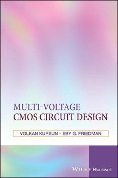
This book presents an in-depth treatment of various power reduction and speed enhancement techniques based on multiple supply and threshold voltages. A detailed discussion of the sources of power consumption in CMOS circuits will be provided whilst focusing primarily on identifying the mechanisms by which sub-threshold and gate oxide leakage currents are generated. The authors present a comprehensive review of state-of-the-art dynamic, static supply and threshold voltage scaling techniques and discuss the pros and cons of supply and threshold voltage scaling techniques.
Andere Kunden interessierten sich auch für
![Low-Voltage Soi CMOS VLSI Devices and Circuits Low-Voltage Soi CMOS VLSI Devices and Circuits]() James B. KuoLow-Voltage Soi CMOS VLSI Devices and Circuits203,99 €
James B. KuoLow-Voltage Soi CMOS VLSI Devices and Circuits203,99 €![Nano-CMOS Design for Manufacturability Nano-CMOS Design for Manufacturability]() Ban P. WongNano-CMOS Design for Manufacturability160,99 €
Ban P. WongNano-CMOS Design for Manufacturability160,99 €![Synthesis of Arithmetic Circuits Synthesis of Arithmetic Circuits]() Jean-Pierre DeschampsSynthesis of Arithmetic Circuits227,99 €
Jean-Pierre DeschampsSynthesis of Arithmetic Circuits227,99 €![Nano-CMOS Circuit and Physical Design Nano-CMOS Circuit and Physical Design]() Ban WongNano-CMOS Circuit and Physical Design221,99 €
Ban WongNano-CMOS Circuit and Physical Design221,99 €![Telecommunication Circuit Design Telecommunication Circuit Design]() Patrick Van der PuijeTelecommunication Circuit Design160,99 €
Patrick Van der PuijeTelecommunication Circuit Design160,99 €![Device Modeling for Analog and RF CMOS Circuit Design Device Modeling for Analog and RF CMOS Circuit Design]() Trond YtterdalDevice Modeling for Analog and RF CMOS Circuit Design208,99 €
Trond YtterdalDevice Modeling for Analog and RF CMOS Circuit Design208,99 €![Mixed-Signal Systems Mixed-Signal Systems]() Andrzej HandkiewiczMixed-Signal Systems202,99 €
Andrzej HandkiewiczMixed-Signal Systems202,99 €-
-
-
This book presents an in-depth treatment of various power reduction and speed enhancement techniques based on multiple supply and threshold voltages. A detailed discussion of the sources of power consumption in CMOS circuits will be provided whilst focusing primarily on identifying the mechanisms by which sub-threshold and gate oxide leakage currents are generated. The authors present a comprehensive review of state-of-the-art dynamic, static supply and threshold voltage scaling techniques and discuss the pros and cons of supply and threshold voltage scaling techniques.
Hinweis: Dieser Artikel kann nur an eine deutsche Lieferadresse ausgeliefert werden.
Hinweis: Dieser Artikel kann nur an eine deutsche Lieferadresse ausgeliefert werden.
Produktdetails
- Produktdetails
- Verlag: Wiley & Sons
- 1. Auflage
- Seitenzahl: 242
- Erscheinungstermin: 1. Oktober 2006
- Englisch
- Abmessung: 251mm x 174mm x 20mm
- Gewicht: 610g
- ISBN-13: 9780470010235
- ISBN-10: 0470010231
- Artikelnr.: 20894845
- Herstellerkennzeichnung
- Libri GmbH
- Europaallee 1
- 36244 Bad Hersfeld
- gpsr@libri.de
DR VOLKAN KURSUN, Department of Electrical & Computer Engineering, University of Rochester, Rochester, New York 14627-0231, USA. PROFESSOR DR EBY G. FRIEDMAN, Department of Electrical & Computer Engineering , University of Rochester , Rochester, New York 14627-0231, USA.
About the Authors xi
Preface xiii
Acknowledgments xv
Chapter 1 Introduction 1
1.1 Evolution of Integrated Circuits 3
1.2 Outline of the Book 14
Chapter 2 Sources of Power Consumption in CMOS ICs 19
2.1 Dynamic Switching Power 19
2.2 Leakage Power 22
2.2.1 Subthreshold Leakage Current 22
2.2.1.1 Short-Channel Effects 23
2.2.1.2 Drain-Induced Barrier-Lowering 25
2.2.1.3 Characterization of Subthreshold Leakage Current 25
2.2.2 Gate Oxide Leakage Current 28
2.2.2.1 Effect of Technology Scaling on Gate Oxide Leakage 29
2.2.2.2 Characterization of Gate Oxide Leakage Current 32
2.2.2.3 Alternative Gate Dielectric Materials 38
2.3 Short-Circuit Power 39
2.4 Static DC Power 43
Chapter 3 Supply and Threshold Voltage Scaling Techniques 45
3.1 Dynamic Supply Voltage Scaling 48
3.2 Multiple Supply Voltage CMOS 51
3.3 Threshold Voltage Scaling 54
3.3.1 Body Bias Techniques 58
3.3.1.1 Reverse Body Bias 58
3.3.1.2 Forward Body Bias 64
3.3.1.3 Bidirectional Body Bias 71
3.3.2 Multiple Threshold Voltage CMOS 74
3.4 Multiple Supply and Threshold Voltage CMOS 77
3.5 Dynamic Supply and Threshold Voltage Scaling 80
3.6 Circuits with Multiple Voltage and Clock Domains 81
3.7 Summary 83
Chapter 4 Low-Voltage Power Supplies 85
4.1 Linear DC-DC Converters 87
4.2 Switched-Capacitor DC-DC Converters 90
4.3 Switching DC-DC Converters 91
4.3.1 Operation of a Buck Converter 92
4.3.2 Power Reduction Techniques for Switching DC-DC Converters 95
4.4 Summary 95
Chapter 5 Buck Converters for On-Chip Integration 99
5.1 Circuit Model of a Buck Converter 101
5.1.1 MOSFET-Related Power Losses 101
5.1.2 Filter Inductor-Related Power Losses 103
5.1.3 Filter Capacitor-Related Power Losses 103
5.1.4 Total Power Consumption of a Buck Converter 104
5.2 Efficiency Analysis of a Buck Converter 104
5.2.1 Circuit Analysis for Global Maximum Efficiency 105
5.2.2 Circuit Analysis with Limited Filter Capacitance 108
5.2.3 Output Voltage Ripple Constraint 109
5.3 Simulation Results 109
5.4 Summary 112
Chapter 6 Low-Voltage Swing Monolithic DC-DC Conversion 115
6.1 Circuit Model of a Low-Voltage Swing Buck Converter 116
6.1.1 MOSFET Power Dissipation 118
6.1.2 MOSFET Model 119
6.1.3 Filter Inductor Power Dissipation 120
6.2 Low-Voltage Swing Buck Converter Analysis 121
6.2.1 Full Swing Circuit Analysis for Global Maximum Efficiency 121
6.2.2 Low Swing Circuit Analysis for Global Maximum Efficiency 123
6.3 Summary 126
Chapter 7 High Input Voltage Step-Down DC-DC Converters 127
7.1 Cascode Bridge Circuits 129
7.1.1 Cascode Bridge Circuit for Input Voltages up to 2Vmax 129
7.1.2 Cascode Bridge Circuit for Input Voltages up to 3Vmax 130
7.1.3 Cascode Bridge Circuit for Input Voltages up to 4Vmax 132
7.2 High Input Voltage Monolithic Switching DC-DC Converters 133
7.2.1 Operation of Cascode DC-DC Converters 133
7.2.2 Efficiency Characteristics of DC-DC Converters Operating at Input
Voltages up to 2Vmax 136
7.2.3 Efficiency Characteristics of DC-DC Converters Operating at Input
Voltages up to 3Vmax 137
7.3 Summary 138
Chapter 8 Signal Transfer in ICs with Multiple Supply Voltages 139
8.1 A High-Speed and Low-Power Voltage Interface Circuit 140
8.2 Voltage Interface Circuit Simulation Results 141
8.3 Experimental Results 144
8.4 Summary 146
Chapter 9 Domino Logic with Variable Threshold Voltage Keeper 147
9.1 Standard Domino (SD) Logic Circuits 148
9.1.1 Operation of Standard Domino Logic Circuits 148
9.1.2 Noise Immunity, Delay, and Energy Tradeoffs 150
9.2 Domino Logic with Variable Threshold Voltage Keeper (DVTVK) 153
9.2.1 Variable Threshold Voltage Keeper 153
9.2.2 Dynamic Body Bias Generator 155
9.3 Simulation Results 156
9.3.1 Multiple-Output Domino Carry Generator with Variable Threshold
Voltage Keeper 156
9.3.1.1 Improved Delay and Power Characteristics with Comparable Noise
Immunity 158
9.3.1.2 Improved Noise Immunity with Comparable Delay or Power
Characteristics 160
9.3.2 Clock-Delayed Domino Logic with Variable Threshold Voltage Keeper 161
9.3.3 Energy Overhead of the Dynamic Body Bias Generator 163
9.4 Domino Logic with Forward and Reverse Body Biased Keeper 164
9.4.1 Clock-Delayed Domino Logic with Forward and Reverse Body Biased
Keeper 165
9.4.2 Technology Scaling Characteristics of the Reverse and Forward Body
Bias Techniques Applied to a Keeper Transistor 168
9.5 Summary 169
Chapter 10 Subthreshold Leakage Current Characteristics of Dynamic Circuits
171
10.1 State-Dependent Subthreshold Leakage Current Characteristics 172
10.2 Noise Immunity 177
10.3 Power and Delay Characteristics in the Active Mode 180
10.4 Dual Threshold Voltage CMOS Technology 182
10.5 Summary 186
Chapter 11 Sleep Switch Dual Threshold Voltage Domino Logic 187
11.1 Existing Sleep Mode Circuit Techniques 188
11.2 Dual Threshold Voltage Domino Logic Employing Sleep Switches 190
11.3 Simulation Results 191
11.3.1 Subthreshold Leakage Energy Reduction 193
11.3.2 Stack Effect in Domino Logic Circuits 194
11.3.3 Delay and Power Reduction in the Active Mode 197
11.3.4 Sleep/Wake-Up Delay and Energy Overhead 197
11.4 Noise Immunity Compensation 200
11.5 Summary 204
Chapter 12 Conclusions 205
Bibliography 211
Index 221

