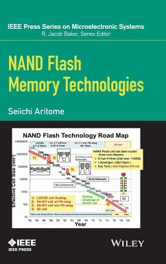
Seiichi Aritome
Nand Flash Memory Technologies
Seiichi Aritome
Nand Flash Memory Technologies
- Gebundenes Buch
- Merkliste
- Auf die Merkliste
- Bewerten Bewerten
- Teilen
- Produkt teilen
- Produkterinnerung
- Produkterinnerung
_ Offers a comprehensive overview of NAND flash memories, with insights into NAND history, technology, challenges, evolutions, and perspectives _ Describes new program disturb issues, data retention, power consumption, and possible solutions for the challenges of 3D NAND flash memory _ Written by an authority in NAND flash memory technology, with over 25 years' experience
Andere Kunden interessierten sich auch für
![Inside NAND Flash Memories Inside NAND Flash Memories]() Rino MicheloniInside NAND Flash Memories172,99 €
Rino MicheloniInside NAND Flash Memories172,99 €![Nonvolatile Memory Technologies with Emphasis on Flash Nonvolatile Memory Technologies with Emphasis on Flash]() Nonvolatile Memory Technologies with Emphasis on Flash203,99 €
Nonvolatile Memory Technologies with Emphasis on Flash203,99 €![Junctionless Field-Effect Transistors Junctionless Field-Effect Transistors]() Shubham SahayJunctionless Field-Effect Transistors135,99 €
Shubham SahayJunctionless Field-Effect Transistors135,99 €![ARC Flash Hazard Analysis and Mitigation ARC Flash Hazard Analysis and Mitigation]() J. C. DasARC Flash Hazard Analysis and Mitigation140,99 €
J. C. DasARC Flash Hazard Analysis and Mitigation140,99 €![Embedded Flash Memory for Embedded Systems: Technology, Design for Sub-systems, and Innovations Embedded Flash Memory for Embedded Systems: Technology, Design for Sub-systems, and Innovations]() Embedded Flash Memory for Embedded Systems: Technology, Design for Sub-systems, and Innovations67,99 €
Embedded Flash Memory for Embedded Systems: Technology, Design for Sub-systems, and Innovations67,99 €![Understanding Delta-SIGMA Data Converters Understanding Delta-SIGMA Data Converters]() Shanthi PavanUnderstanding Delta-SIGMA Data Converters136,99 €
Shanthi PavanUnderstanding Delta-SIGMA Data Converters136,99 €![Flash Memories Flash Memories]() Detlev RichterFlash Memories75,99 €
Detlev RichterFlash Memories75,99 €-
-
-
_ Offers a comprehensive overview of NAND flash memories, with insights into NAND history, technology, challenges, evolutions, and perspectives
_ Describes new program disturb issues, data retention, power consumption, and possible solutions for the challenges of 3D NAND flash memory
_ Written by an authority in NAND flash memory technology, with over 25 years' experience
_ Describes new program disturb issues, data retention, power consumption, and possible solutions for the challenges of 3D NAND flash memory
_ Written by an authority in NAND flash memory technology, with over 25 years' experience
Produktdetails
- Produktdetails
- IEEE Press Series on Microelectronic Systems
- Verlag: Wiley & Sons / Wiley-IEEE Press
- Artikelnr. des Verlages: 1W119132600
- 1. Auflage
- Seitenzahl: 432
- Erscheinungstermin: 29. Dezember 2015
- Englisch
- Abmessung: 240mm x 161mm x 28mm
- Gewicht: 812g
- ISBN-13: 9781119132608
- ISBN-10: 1119132606
- Artikelnr.: 43037776
- Herstellerkennzeichnung
- Libri GmbH
- Europaallee 1
- 36244 Bad Hersfeld
- gpsr@libri.de
Seiichi Aritome was a Senior Research Fellow at SK Hynix Inc. in Icheon, Korea from 2009 to 2014. He has contributed to NAND flash memory technologies for over 27 years in several companies and nations. Aritome was a Program director at Powerchip Semiconductor Corp. in Hsinchu, Taiwan, a Senior Process Reliability Engineer at Micron Technology Inc. in Idaho, USA, and a Chief Specialist at Toshiba Corporation in Kawasaki, Japan. He received his Ph.D. from Graduate School of Advanced Sciences of Matter, Hiroshima University, Japan. Aritome is an IEEE Fellow and a member of the IEEE Electron Device Society.
Foreword xi
Preface xv
Acknowledgments xvii
About the Author xix
1 Introduction 1
1.1 Background, 1
1.2 Overview, 8
References, 10
2 Principle of NAND Flash Memory 17
2.1 NAND Flash Device and Architecture, 17
2.1.1 NAND Flash Memory Cell Architecture, 17
2.1.2 Peripheral Device, 19
2.2 Cell Operation, 21
2.2.1 Read Operation, 21
2.2.2 Program and Erase Operation, 21
2.2.3 Program and Erase Dynamics, 28
2.2.4 Program Boosting Operation, 31
2.3 Multilevel Cell (MLC), 34
2.3.1 Cell Vt Setting, 34
References, 35
3 NAND Flash Memory Devices 37
3.1 Introduction, 37
3.2 LOCOS Cell, 40
3.2.1 Conventional LOCOS Cell, 40
3.2.2 Advanced LOCOS Cell, 40
3.2.3 Isolation Technology, 43
3.2.4 Reliability, 46
3.3 Self-Aligned STI Cell (SA-STI Cell) with FG Wing, 48
3.3.1 Structure of SA-STI Cell, 48
3.3.2 Fabrication Process Flow, 50
3.3.3 Characteristics of SA-STI with FG Wing Cell, 53
3.3.4 Characteristics of Peripheral Devices, 57
3.4 Self-Aligned STI Cell (SA-STI Cell) without FG Wing, 59
3.4.1 SA-STI Cell Structure, 59
3.4.2 Fabrication Process, 60
3.4.3 Shallow Trench Isolation (STI), 61
3.4.4 SA-STI Cell Characteristics, 64
3.5 Planar FG Cell, 66
3.5.1 Structure Advantages, 66
3.5.2 Electrical Characteristics, 68
3.6 Sidewall Transfer Transistor Cell (SWATT Cell), 69
3.6.1 Concept of the SWATT Cell, 70
3.6.2 Fabrication Process, 71
3.6.3 Electrical Characteristics, 74
3.7 Advanced NAND Flash Device Technologies, 77
3.7.1 Dummy Word Line, 77
3.7.2 The P-Type Floating Gate, 82
References, 89
4 Advanced Operation for Multilevel Cell 93
4.1 Introduction, 93
4.2 Program Operation for Tight Vt Distribution Width, 94
4.2.1 Cell Vt Setting, 94
4.2.2 Incremental Step Pulse Program (ISPP), 95
4.2.3 Bit-by-Bit Verify Operations, 98
4.2.4 Two-Step Verify Scheme, 99
4.2.5 Pseudo-Pass Scheme in Page Program, 102
4.3 Page Program Sequence, 104
4.3.1 Original Page Program Scheme, 104
4.3.2 New Page Program Scheme (1), 107
4.3.3 New Page Program Scheme (2), 108
4.3.4 All-Bit-Line (ABL) Architecture, 111
4.4 TLC (3 Bits/Cell), 113
4.5 QLC (4 Bits/Cell), 115
4.6 Three-Level (1.5 Bits/Cell) NAND flash, 119
4.7 Moving Read Algorithm, 122
References, 123
5 Scaling Challenge of NAND Flash Memory Cells 129
5.1 Introduction, 129
5.2 Read Window Margin (RWM), 130
5.2.1 Assumption for Read Window Margin (RWM), 131
5.2.2 Programmed Vt Distribution Width, 135
5.2.3 Vt Window, 137
5.2.4 Read Window Margin (RWM), 139
5.2.5 RWM Vt Setting Dependence, 140
5.3 Floating-Gate Capacitive Coupling Interference, 142
5.3.1 Model of Floating-Gate Capacitive Coupling Interference, 142
5.3.2 Direct Coupling with Channel, 145
5.3.3 Coupling with Source/Drain, 148
5.3.4 Air Gap and Low-k Material, 149
5.4 Program Electron Injection Spread, 153
5.4.1 Theory of Program Electron Injection Spread, 153
5.4.2 Effect of Lower Doping in FG, 158
5.5 Random Telegraph Signal Noise (RTN), 161
5.5.1 RTN in Flash Memory Cells, 161
&

