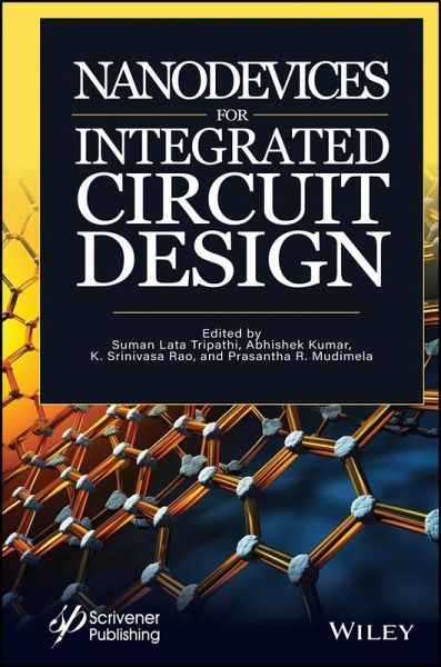
Nanodevices are an integral part of many of the technologies that we use every day. It is a constantly changing and evolving area, with new materials, processes, and applications coming online almost daily. Increasing demand for smart and intelligent devices in human life with better sensing, communication and signal processing is increasingly pushing researchers and designers towards future design challenges based upon internet-of-things (IoT) applications. Several types of research have been done at the level of solid-state devices, circuits, and materials to optimize system performance with…mehr
Nanodevices are an integral part of many of the technologies that we use every day. It is a constantly changing and evolving area, with new materials, processes, and applications coming online almost daily. Increasing demand for smart and intelligent devices in human life with better sensing, communication and signal processing is increasingly pushing researchers and designers towards future design challenges based upon internet-of-things (IoT) applications. Several types of research have been done at the level of solid-state devices, circuits, and materials to optimize system performance with low power consumption. For suitable IoT-based systems, there are some key areas, such as the design of energy storage devices, energy harvesters, novel low power high-speed devices, and circuits. Uses of new materials for different purposes, such as semiconductors, metals, and insulators in different parts of devices, circuits, and energy sources, also play a significant role in smart applications of such systems. Emerging techniques like machine learning and artificial intelligence are also becoming a part of the latest developments in an electronic device and circuit design. This groundbreaking new book will, among other things, aid developing countries in updating their semiconductor industries in terms of IC design and manufacturing to avoid dependency on other countries. Likewise, as an introduction to the area for the new-hire or student, and as a reference for the veteran engineer in the field, it will be helpful for more developed countries in their pursuit of better IC design. It is a must have for any engineer, scientist, or other industry professional working in this area.Hinweis: Dieser Artikel kann nur an eine deutsche Lieferadresse ausgeliefert werden.
Suman Lata Tripathi, PhD, is a professor at Lovely Professional University with more than 21 years of experience in academics. She has published more than 103 research papers in refereed journals and conferences. She has organized several workshops, summer internships, and expert lectures for students, and she has worked as a session chair, conference steering committee member, editorial board member, and reviewer for IEEE journals and conferences. She has published three books and currently has multiple volumes scheduled for publication from Wiley-Scrivener. Abhishek Kumar, PhD, is an associate professor at and obtained his PhD in the area of VLSI Design for Low Power and Secured Architecture from Lovely Professional University, India. With over 11 years of academic experience, he has published more than 30 research papers and proceedings in scholarly journals. He has also published nine book chapters and one authored book. He has worked as a reviewer and program committee member and editorial board member for academic and scholarly conferences and journals, and he has 11 patents to his credit. K. Srinivasa Rao, PhD, is a professor and Head of Microelectronics Research Group, Department of Electronics and Communication Engineering at the Koneru Lakshmaiah Education Foundation, India. He has earned multiple awards for his scholarship and has published more than 150 papers in scientific journals and presented more than 55 papers at scientific conferences around the world. Prasantha R. Mudimela, PhD, is a professor in the Department of Electronics and Communication Engineering, GITAM (deemed to be University), Hyderabad campus, India. He has two years of postdoc experience from the University of Namur, Belgium and KAUST, Saudi Arabia. He has over 15 years of teaching and research experience, and he has published over 45 refereed journal and conference papers.
Inhaltsangabe
List of Contributors xiii Preface xvii Acknowledgements xix 1 Growth of Nano-Wire Field Effect Transistor in 21st Century 1 Kunal Sinha 1.1 Introduction 2 1.2 Initial Works on Nanowire Field-Effect-Transistors (NW-FET) 3 1.2(A) Theoretical and Simulation Studies on Nanowire FET (NW-FET) 4 1.2(B) Fabrication of Nanowire Field-Effect-Transistor (NW-FET) 10 1.3 Application of Nanowire Field-Effect-Transistors (NW-FET) 15 1.4 Conclusion 17 2 Impact of Silicon Nanowire-Based Transistor in IC Design Perspective 23 G. Boopathi Raja 2.1 Introduction 24 2.2 Nanoscale Devices 25 2.3 Nanowire Heterostructures and Silicon Nanowires 29 2.4 Performance Analysis of Si Nanowire with SOI FET 38 2.5 Conclusion 40 3 Kink Effect in Field Effect Transistors: Different Models and Techniques 43 Abdelaali Fargi, Sami Ghedira and Adel Kalboussi 3.1 Introduction 44 3.2 Techniques of Kink Effect 45 3.3 Different Models of Kink Effect 48 3.4 Kink Effect in MOS Capacitors 48 3.5 Conclusion 58 4 Next Generation Molybdenum Disulfide FET: Its Properties, Evaluation, and Its Applications 61 Vydha Pradeep Kumar and Deepak Kumar Panda 4.1 Introduction of Two-Dimensional Materials 62 4.2 Evaluation of 2D-Materials 64 4.3 Overview of MoS2 66 4.4 Properties of MoS2 68 4.5 Fabrication of MoS2 71 4.6 Applications of MoS2 72 4.7 Comparison of Other 2D Materials with MoS2 75 4.8 Conclusion 80 5 Impact of Working Temperature on the ION /IOFF Ratio of a Hetero Step-Shaped Gate TFET With Improved Ambipolar Conduction 83 Bijoy Goswami, Savio Jay Sengupta, Ankur Jyoti Sarmah and Nalin Behari Dev Choudhury 5.1 Introduction 84 5.2 Device Structure 84 5.3 Results and Discussion 86 5.4 Conclusion 89 6 Analysis of RF with DC and?@Linearity Parameter and Study of Noise Characteristics of Gate-All-Around Junctionless FET (GAA-JLFET) and Its Applications 93 Pratikhya Raut, Umakanta Nanda and Deepak Kumar Panda 6.1 Introduction 94 6.2 Structure of GAA-JLFET 97 6.3 Results and Discussion 98 6.4 Applications 112 6.5 Conclusion 112 7 E-Mode-Operated Advanced III-V Heterostructure Quantum Well Devices for Analog/RF and High-Power Switching Applications 117 A. Mohanbabu, N. Vinodhkumar, S. Maheswari, S. Baskaran, V. Janakiraman, M. Saravanan and P. Murugapandiyan 7.1 Silicon Era and Scaling Limit 118 7.2 III-V GaN-Based Compound Semiconductors 119 7.3 Band-Gap Engineering 119 7.4 Quantum Well 120 7.5 Polarization in GaN Devices and their Specific Properties 121 7.6 Strain and Lattice Mismatch in III-N Semiconductors 123 7.7 High Electron Mobility Transistors (HEMTs) 123 7.8 Two-Dimensional Electron Gas (2DEG) 124 7.9 AlGaN/GaN Heterostructure HEMT 125 7.10 Enhancement Mode GaN DH-HEMTs Device With Boron-Doped Gate Cap Layer 129 7.11 High-K Gate Dielectric III-Nitride GaN MIS-HEMT Devices 132 7.12 Conclusion 137 8 Design of FinFET as Biosensor 143 Suman Lata Tripathi and Balwinder Raj 8.1 Introduction 143 8.2 Existing FET Based Biosensors 145 8.3 Performance Parameters of Biosensors 149 8.4 FinFET Designed as Biosensor Using Visual TCAD 149 8.5 Biosensors in Disease Detection 152 8.6 Conclusion 153 8.7 Acknowledgement 154 9 Biodegradable and Flexible Electronics: Types and Applications 157 Vrinda Gupta, Sachin Himalyan and Archit Sundriyal 9.1 Introduction 158 9.2 Biodegradable and Flexible Electronics 160 9.3 Types of Materials Used for Biodegradable and Flexible Electronics 164 9.4 Applications of Biodegradable and Flexible Electronic Devices 171 9.5 Conclusion 176 10 Novel Parameters Extraction Method of High-Speed PIN Diode for Power Integrated Circuit 181 Sami Ghedira and Abdelaali Fargi 10.1 Introduction 182 10.2 Review of the Technology and Physics of Power PIN Diodes 183 10.3 State of the Art of PIN Diode Parameters Extraction 186 10.4 Proposed Method 188 10.5 Validation 205 10.6 Conclusion 207 11 Edge AI -- A Promising Technology 211 Remya R., Nalesh S. and Kala S. 11.1 Introduction 211 11.2 Deep Neural Networks 213 11.3 Model Compression Techniques for Deep Learning 216 11.4 Computing Infrastructures 221 11.5 Conclusion 223 12 Tunable Frequency Oscillator 227 Abhishek Kumar 12.1 Introduction 227 12.2 Experimental Methods and Materials 230 12.3 Results and Discussion 235 12.4 Conclusion 240 13 Introduction to Nanomagnetic Materials for Electronic Devices: Fundamental, Synthesis, Classification and Applications 243 Shivani Malhotra, Mansi Chitkara, Lipika Gupta and Monika Parmar 13.1 Introduction -- An Explanation of the Process and Approach 244 13.2 Nanomaterials 244 13.3 Synthesis and Characterization of Nano Materials 248 13.4 Characterization Technique for Structural Analysis 251 13.5 Magnetic Materials 252 13.6 Classification of Magnetic Materials 253 13.7 Magnetic Properties 256 13.8 Ferrites 258 13.9 Applications of Magnetic Materials 265 13.10 Conclusion 268 References 268 About the Editors 273 Index 275
Es gelten unsere Allgemeinen Geschäftsbedingungen: www.buecher.de/agb
Impressum
www.buecher.de ist ein Internetauftritt der buecher.de internetstores GmbH
Geschäftsführung: Monica Sawhney | Roland Kölbl | Günter Hilger
Sitz der Gesellschaft: Batheyer Straße 115 - 117, 58099 Hagen
Postanschrift: Bürgermeister-Wegele-Str. 12, 86167 Augsburg
Amtsgericht Hagen HRB 13257
Steuernummer: 321/5800/1497
USt-IdNr: DE450055826