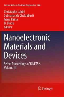
Nanoelectronic Materials and Devices
Select Proceedings of ICNETS2, Volume III
Herausgegeben:Labbé, Christophe; Chakrabarti, Subhananda; Raina, Gargi; Bindu, B.
Nanoelectronic Materials and Devices
Select Proceedings of ICNETS2, Volume III
Herausgegeben:Labbé, Christophe; Chakrabarti, Subhananda; Raina, Gargi; Bindu, B.
- Broschiertes Buch
- Merkliste
- Auf die Merkliste
- Bewerten Bewerten
- Teilen
- Produkt teilen
- Produkterinnerung
- Produkterinnerung
This book gathers a collection of papers by international experts that were presented at the International Conference on NextGen Electronic Technologies (ICNETS2-2016). ICNETS2 encompassed six symposia covering all aspects of the electronics and communications domains, including relevant nano/micro materials and devices. Highlighting the latest research on nanoelectronic materials and devices, the book offers a valuable guide for researchers, practitioners and students working in the core areas of functional electronics nanomaterials, nanocomposites for energy application, sensing and high…mehr
Andere Kunden interessierten sich auch für
![Nanoelectronic Materials and Devices Nanoelectronic Materials and Devices]() Nanoelectronic Materials and Devices154,99 €
Nanoelectronic Materials and Devices154,99 €![Functional Nanostructures and Metamaterials for Superconducting Spintronics Functional Nanostructures and Metamaterials for Superconducting Spintronics]() Functional Nanostructures and Metamaterials for Superconducting Spintronics100,99 €
Functional Nanostructures and Metamaterials for Superconducting Spintronics100,99 €![Freshman Lectures on Nanotechnology Freshman Lectures on Nanotechnology]() Hassan RazaFreshman Lectures on Nanotechnology35,99 €
Hassan RazaFreshman Lectures on Nanotechnology35,99 €![Functional Nanostructures and Metamaterials for Superconducting Spintronics Functional Nanostructures and Metamaterials for Superconducting Spintronics]() Functional Nanostructures and Metamaterials for Superconducting Spintronics100,99 €
Functional Nanostructures and Metamaterials for Superconducting Spintronics100,99 €![Nanoelectronics Fundamentals Nanoelectronics Fundamentals]() Hassan RazaNanoelectronics Fundamentals154,99 €
Hassan RazaNanoelectronics Fundamentals154,99 €![The Wigner Monte Carlo Method for Nanoelectronic Devices The Wigner Monte Carlo Method for Nanoelectronic Devices]() Damien QuerliozThe Wigner Monte Carlo Method for Nanoelectronic Devices187,99 €
Damien QuerliozThe Wigner Monte Carlo Method for Nanoelectronic Devices187,99 €![Polyvinyl Alcohol/Halloysite Nanotube Bionanocomposites as Biodegradable Packaging Materials Polyvinyl Alcohol/Halloysite Nanotube Bionanocomposites as Biodegradable Packaging Materials]() Zainab Waheed AbdullahPolyvinyl Alcohol/Halloysite Nanotube Bionanocomposites as Biodegradable Packaging Materials100,99 €
Zainab Waheed AbdullahPolyvinyl Alcohol/Halloysite Nanotube Bionanocomposites as Biodegradable Packaging Materials100,99 €-
-
-
This book gathers a collection of papers by international experts that were presented at the International Conference on NextGen Electronic Technologies (ICNETS2-2016). ICNETS2 encompassed six symposia covering all aspects of the electronics and communications domains, including relevant nano/micro materials and devices. Highlighting the latest research on nanoelectronic materials and devices, the book offers a valuable guide for researchers, practitioners and students working in the core areas of functional electronics nanomaterials, nanocomposites for energy application, sensing and high strength materials and simulation of novel device design structures for ultra-low power applications.
Produktdetails
- Produktdetails
- Lecture Notes in Electrical Engineering 466
- Verlag: Springer / Springer Nature Singapore / Springer, Berlin
- Artikelnr. des Verlages: 978-981-13-5602-5
- Softcover reprint of the original 1st ed. 2018
- Seitenzahl: 260
- Erscheinungstermin: 25. Dezember 2018
- Englisch
- Abmessung: 235mm x 155mm x 14mm
- Gewicht: 480g
- ISBN-13: 9789811356025
- ISBN-10: 9811356025
- Artikelnr.: 54771586
- Herstellerkennzeichnung Die Herstellerinformationen sind derzeit nicht verfügbar.
Dr. Christophe Labbé is an Associate Professor at CIMAP Lab (Centre de Recherche sur les Ions, les Matériaux et la Photonique) at Caen, France in the engineering school ENSICAEN. He obtained his PhD on rare earth lasers at the Interdisciplinary Research Center Laser Ions at Caen in 1999. After a postgraduate position in Israel at the Laser Arava Laboratory of the Ben-Gurion University of the Negev, Israel on ionic matrix lasers pumped by diode, he became an assistant professor at the Laboratory of Optical Functions for Telecommunications (FOTON Lab) in Rennes, France in 2002. His ongoing research focuses on photon sources for telecommunications or visible light applications, and on photovoltaic cells. Dr. Subhananda Chakrabarti received his MSc and PhD degrees from the Department of Electronic Science, University of Calcutta, India in 1993 and 2000, respectively. He was a Lecturer at the Department of Physics, St. Xavier's College, Kolkata. He served as a SeniorResearch Fellow with the University of Michigan, Ann Arbor, USA from 2001 to 2005, as a Senior Researcher with Dublin City University, Ireland, from 2005 to 2006, and as a Senior Researcher (RA2) with the University of Glasgow, UK, from 2006 to 2007. He became an Assistant Professor at the Department of Electrical Engineering, Indian Institute of Technology Bombay (IIT Bombay), India, in 2007, where he currently serves as a Professor. He is a Fellow of the Institution of Electrical and Telecommunication Engineers (IETE) India and a Member of the IEEE, MRS USA, SPIE USA etc. His research interests lie in compound (III-V and II-VI) semiconductor-based optoelectronic materials and devices. Prof. (Dr.) Gargi Raina is a Professor at the School of Electronics Engineering (SENSE), VIT University, India. She completed her MS in Condensed Matter Physics at the Department of Physics and Astronomy, University of Hawaii at Manoa, USA (1991). She obtained her PhD from Jawaharlal Nehru Centre for Advanced Scientific Research (JNCASR), Bangalore, India in 2004. She worked as an "Application Scientist" and helped set up the Advanced Metrology Application Lab of Digital Instruments/Veeco Inc., USA at JNCASR, Bangalore. She joined the Vellore Institute of Technology in 2006 as an Associate Professor and has been a Professor since 2008, while also serving as Director of the Center for Nanotechnology Research from June 2014 to September 2015. Her current research interests include functional nanomaterials, nanopatterning and assembly techniques, scanning probe microscopy (SPM)-based nanolithography, patterning and Lithography for graphene, graphene and nanocarbon materials for energy applications, simulation of carbon nanotube (CNT)/graphene-based nanoscale devices, and plasmonic nanolithography. Dr. B. Bindu received her MTech in Digital Electronics from Cochin University of Science and Technology, India and Ph.D. in Electrical Engineering from the Indian Institute of Technology Madras (IIT Madras), Chennai, India. Her specialization is in nanoelectronics and very-large-scale integration (VLSI). She worked as a postdoctoral researcher for three years with the Device Modelling Group, University of Glasgow, UK and with the Institute for Microelectronics, Technical University Vienna, Austria. Currently, she is an Associate Professor at VIT University, Chennai. Her current research interests include the modelling of various issues in nanoscaled metal-oxide semiconductor field-effect transistors (MOSFETs), compact modelling of non-classical MOSFETs, and power semiconductor devices for analog and digital VLSI circuit design.
The Effect of Functionalized MWCNT on Mechanical and Electrical Properties of PMMA Nanocomposites.- Performance Analysis of Dual-Metal Double-Gate Tunnel-Fets for Ultralow Power Applications.- Films of Reduced Graphene Oxide based Metal Oxide Nanoparticles.- Size optimization of InAs/GaAs quantum dots for longer storage memory applications.- Design and Analysis of a CMOS 180 nm Fractional N Frequency Synthesizer.- Memristor based Approximate Adders for Error Resilient Applications.- Integrated Mems Capacitive Pressure Sensor with On-Chip CDC for a wide Operating Temperature Range.- A High SNDR and Wider Signal Bandwidth CT Modulator with a Single Loop Non-linear Feedback Compensation.- Design of Current Mode CNTFET Transceiver for Bundled Carbon Nanotube Interconnect.- Weak Cell Detection Techniques for Memristor Based Memories.- Enhancement of Transconductance using Multi-recycle Folded Cascode Amplifier.- Nondestructive Read Circuit for Memristor based Memories.- A Built in Self Repair Architecture for Random Access Memories.- A Current Mode DC-DC Boost Converter with Fast Transient and on-chip Current Sensing Technique.- A Modified GDI Based Low Power & High Read Stability 8T SRAM Memory with CNTFET Technology.- High Performance Trench Gate Power MOSFET of Indium Phosphide.- Memristor Equipped Error Detection Technique.- 28nm FD-SOI SRAM Design using Read Stable Bit Cell Architecture.- Design and Verification of Memory Controller with Host WISHBONE Interface.- 8-Bit Asynchronous Wave-Pipelined Arithmetic-Logic Unit.
The Effect of Functionalized MWCNT on Mechanical and Electrical Properties of PMMA Nanocomposites.- Performance Analysis of Dual-Metal Double-Gate Tunnel-Fets for Ultralow Power Applications.- Films of Reduced Graphene Oxide based Metal Oxide Nanoparticles.- Size optimization of InAs/GaAs quantum dots for longer storage memory applications.- Design and Analysis of a CMOS 180 nm Fractional N Frequency Synthesizer.- Memristor based Approximate Adders for Error Resilient Applications.- Integrated Mems Capacitive Pressure Sensor with On-Chip CDC for a wide Operating Temperature Range.- A High SNDR and Wider Signal Bandwidth CT Modulator with a Single Loop Non-linear Feedback Compensation.- Design of Current Mode CNTFET Transceiver for Bundled Carbon Nanotube Interconnect.- Weak Cell Detection Techniques for Memristor Based Memories.- Enhancement of Transconductance using Multi-recycle Folded Cascode Amplifier.- Nondestructive Read Circuit for Memristor based Memories.- A Built in Self Repair Architecture for Random Access Memories.- A Current Mode DC-DC Boost Converter with Fast Transient and on-chip Current Sensing Technique.- A Modified GDI Based Low Power & High Read Stability 8T SRAM Memory with CNTFET Technology.- High Performance Trench Gate Power MOSFET of Indium Phosphide.- Memristor Equipped Error Detection Technique.- 28nm FD-SOI SRAM Design using Read Stable Bit Cell Architecture.- Design and Verification of Memory Controller with Host WISHBONE Interface.- 8-Bit Asynchronous Wave-Pipelined Arithmetic-Logic Unit.

