Nanoelectronics
From Device Physics and Fabrication Technology to Advanced Transistor Concepts

PAYBACK Punkte
30 °P sammeln!
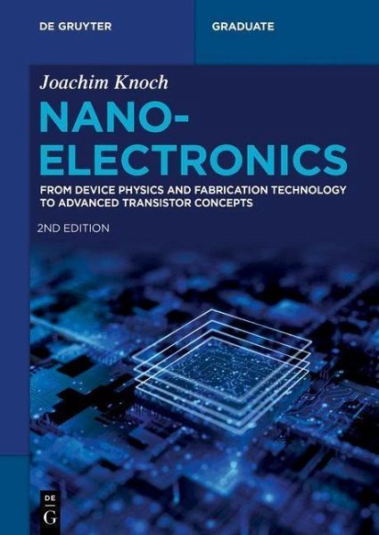
In recent years, nanoelectronics has become very interdisciplinary requiring students to master aspects of physics, electrical engineering, chemistry etc. The 2nd edition of this textbook is a comprehensive overview of nanoelectronics covering the necessary quantum mechanical and solid-state physics foundation, an overview of semiconductor fabrication as well as a brief introduction into device simulation using the non-equilibrium Greens function formalism. Equipped with this, the work discusses nanoscale field-effect transistors and alternative device concepts such as Schottky-barrier MOSFETs...
In recent years, nanoelectronics has become very interdisciplinary requiring students to master aspects of physics, electrical engineering, chemistry etc. The 2nd edition of this textbook is a comprehensive overview of nanoelectronics covering the necessary quantum mechanical and solid-state physics foundation, an overview of semiconductor fabrication as well as a brief introduction into device simulation using the non-equilibrium Greens function formalism. Equipped with this, the work discusses nanoscale field-effect transistors and alternative device concepts such as Schottky-barrier MOSFETs as well as steep slope transistors based on different materials. In addition, cryogenic operation of MOSFETs for the realization of, e.g., classical control electronics of semiconducting spin qubits is studied.
The work contains a number of tasks, examples and exercises with step-by-step video solutions as well as tutorial videos that deepen the understanding of the material. With additional access to simulation tools that allow students to do computational experiments, the emphasis is on thorough explanation of the material enabling students to carry out their own research.
The work contains a number of tasks, examples and exercises with step-by-step video solutions as well as tutorial videos that deepen the understanding of the material. With additional access to simulation tools that allow students to do computational experiments, the emphasis is on thorough explanation of the material enabling students to carry out their own research.


