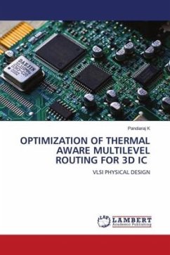
OPTIMIZATION OF THERMAL AWARE MULTILEVEL ROUTING FOR 3D IC
VLSI PHYSICAL DESIGN
Versandkostenfrei!
Versandfertig in 6-10 Tagen
53,99 €
inkl. MwSt.

PAYBACK Punkte
27 °P sammeln!
Very Large Scale Integration (VLSI) is a process of creating an integrated circuit by linking a large number of transistors into a single chip. A 3D IC provides a positive effect on both execution and wirelength in a power system. A three dimensional integrated circuit would become a developing process where connection delays and power get reduced. The several layers of 3D IC which have been linked could be performed by utilizing through silicon via method. It offers better performance than the conventional approach due to decreased length and power consumption. A test access mechanism techniq...
Very Large Scale Integration (VLSI) is a process of creating an integrated circuit by linking a large number of transistors into a single chip. A 3D IC provides a positive effect on both execution and wirelength in a power system. A three dimensional integrated circuit would become a developing process where connection delays and power get reduced. The several layers of 3D IC which have been linked could be performed by utilizing through silicon via method. It offers better performance than the conventional approach due to decreased length and power consumption. A test access mechanism technique has become significant owing to the impact of sinking routing cost. If a large number of TSV has been employed, then it leads to superior area consumption and increases ultimate chip cost. Uneven distribution of TSV is occurred owing to the bonding stratum procedure. It affects not only the area but also wirelength and temperature. At the routing phase, through silicon via could be done by identifying whitespace from integrated circuit system.


