Noboru Kimizuka, Shunpei Yamazaki
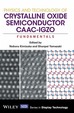
Physics and Technology of Crystalline Oxide Semiconductor Caac-Igzo
Fundamentals
Noboru Kimizuka, Shunpei Yamazaki
Physics and Technology of Crystalline Oxide Semiconductor Caac-Igzo
Fundamentals
- Gebundenes Buch
- Merkliste
- Auf die Merkliste
- Bewerten Bewerten
- Teilen
- Produkt teilen
- Produkterinnerung
- Produkterinnerung
Electronic devices based on oxide semiconductors are the focus of much attention, with crystalline materials generating huge commercial success. Indium-gallium-zinc oxide (IGZO) transistors have a higher mobility than amorphous silicon transistors, and an extremely low off-state current. C-axis aligned crystalline (CAAC) IGZO enables aggressive down-scaling, high reliability, and process simplification of transistors in displays and LSI devices. This original book introduces the CAAC-IGZO structure, and describes the physics and technology of this new class of oxide materials. It explains the…mehr
Andere Kunden interessierten sich auch für
![Physics and Technology of Crystalline Oxide Semiconductor CAAC-IGZO Physics and Technology of Crystalline Oxide Semiconductor CAAC-IGZO]() Physics and Technology of Crystalline Oxide Semiconductor CAAC-IGZO148,99 €
Physics and Technology of Crystalline Oxide Semiconductor CAAC-IGZO148,99 €![Physics and Technology of Crystalline Oxide Semiconductor Caac-Igzo Physics and Technology of Crystalline Oxide Semiconductor Caac-Igzo]() Physics and Technology of Crystalline Oxide Semiconductor Caac-Igzo128,99 €
Physics and Technology of Crystalline Oxide Semiconductor Caac-Igzo128,99 €![Physics and Applications of Non-Crystalline Semiconductors in Optoelectronics Physics and Applications of Non-Crystalline Semiconductors in Optoelectronics]() A. Andriesh / M. Bertolotti (Hgg.)Physics and Applications of Non-Crystalline Semiconductors in Optoelectronics161,99 €
A. Andriesh / M. Bertolotti (Hgg.)Physics and Applications of Non-Crystalline Semiconductors in Optoelectronics161,99 €![ULSI Semiconductor Technology Atlas ULSI Semiconductor Technology Atlas]() Chih-Hang TungULSI Semiconductor Technology Atlas276,99 €
Chih-Hang TungULSI Semiconductor Technology Atlas276,99 €![Photoalignment of Liquid Crystalline Materials Photoalignment of Liquid Crystalline Materials]() Chris K. AtterwillPhotoalignment of Liquid Crystalline Materials151,99 €
Chris K. AtterwillPhotoalignment of Liquid Crystalline Materials151,99 €![Advanced Interconnects for ULSI Technology Advanced Interconnects for ULSI Technology]() Mikhail BaklanovAdvanced Interconnects for ULSI Technology256,99 €
Mikhail BaklanovAdvanced Interconnects for ULSI Technology256,99 €![Physics and Technology of Amorphous-Crystalline Heterostructure Silicon Solar Cells Physics and Technology of Amorphous-Crystalline Heterostructure Silicon Solar Cells]() Physics and Technology of Amorphous-Crystalline Heterostructure Silicon Solar Cells163,99 €
Physics and Technology of Amorphous-Crystalline Heterostructure Silicon Solar Cells163,99 €-
-
-
Electronic devices based on oxide semiconductors are the focus of much attention, with crystalline materials generating huge commercial success. Indium-gallium-zinc oxide (IGZO) transistors have a higher mobility than amorphous silicon transistors, and an extremely low off-state current. C-axis aligned crystalline (CAAC) IGZO enables aggressive down-scaling, high reliability, and process simplification of transistors in displays and LSI devices. This original book introduces the CAAC-IGZO structure, and describes the physics and technology of this new class of oxide materials. It explains the crystallographic classification and characteristics of crystalline oxide semiconductors, their crystallographic characteristics and physical properties, and how this unique material has made a major contribution to the field of oxide semiconductor thin films. Two further books in this series describe applications of CAAC-IGZO in flat-panel displays and LSI devices. Key features: - Introduces the unique and revolutionary, yet relatively unknown crystalline oxide semiconductor CAAC-IGZO - Presents crystallographic overviews of IGZO and related compounds. - Offers an in-depth understanding of CAAC-IGZO. - Explains the fabrication method of CAAC-IGZO thin films. - Presents the physical properties and latest data to support high-reliability crystalline IGZO based on hands-on experience. - Describes the manufacturing process the CAAC-IGZO transistors and introduces the device application using CAAC-IGZO.
Hinweis: Dieser Artikel kann nur an eine deutsche Lieferadresse ausgeliefert werden.
Hinweis: Dieser Artikel kann nur an eine deutsche Lieferadresse ausgeliefert werden.
Produktdetails
- Produktdetails
- Verlag: Wiley
- Seitenzahl: 352
- Erscheinungstermin: 17. Oktober 2016
- Englisch
- Abmessung: 250mm x 175mm x 23mm
- Gewicht: 786g
- ISBN-13: 9781119247401
- ISBN-10: 1119247403
- Artikelnr.: 46002965
- Herstellerkennzeichnung
- Libri GmbH
- Europaallee 1
- 36244 Bad Hersfeld
- gpsr@libri.de
- Verlag: Wiley
- Seitenzahl: 352
- Erscheinungstermin: 17. Oktober 2016
- Englisch
- Abmessung: 250mm x 175mm x 23mm
- Gewicht: 786g
- ISBN-13: 9781119247401
- ISBN-10: 1119247403
- Artikelnr.: 46002965
- Herstellerkennzeichnung
- Libri GmbH
- Europaallee 1
- 36244 Bad Hersfeld
- gpsr@libri.de
Shunpei Yamazaki, Semiconductor Energy Laboratory Co., Ltd., Kanagawa, JAPAN Dr. Shunpei Yamazaki is an authority on semiconductors, memory devices, and liquid crystal displays. Listed on over 4,000 US utility patents, Dr. Yamazaki was named in the Guinness Book of World Records as holding the most patents in the world; hailed the most prolific inventor in history by USA Today (in 2005). His most notable work is on the thin-film transistor -- a significant discovery being a crystalline structure in Indium gallium zinc oxide (IGZO) material, which he discovered "by chance" in 2009. Today Dr. Yamazaki is President of the Semiconductor Energy Laboratory (SEL), where he and his team pioneered the unique development of ultra-low-power devices using CAAC-IGZO technology. A joint venture with the Sharp Corporation manufacturing smartphones using crystalline oxide semiconductors (IGZO) is a global first. In 2015 Dr. Yamazaki received the SID (Society for Information Display) Special Recognition Award for "discovering CAAC-IGZO semiconductors, leading its practical application, and paving the way to next-generation displays." His paper on CAAC-IGZO ranked in the top 15 most downloaded papers of Wiley Electrical Engineering and Communications Technology journals, 2014. Dr. Yamazaki is also an IEEE Life Fellow. Noboru Kimizuka, Kimizuka Institute for Natural Philosophy, Poland Noboru Kimizuka: director of Kimizuka Institute for Natural Philosophy in Poland and adviser of Semiconductor Energy Laboratory, Co., Ltd. He received a Doctor of Science degree from Tokyo Institute of Technology. He joined in the National Institute for Research in Inorganic Materials (NIRIM) of Science and Technology Agency in 1967 (The institute later became the National Institute for Materials Science.) In 1985, he synthesized crystalline IGZO for the first time in the world at NIRIM. Since then, he devoted himself for developing homologous IGZO for about ten years. After he left NIRIM, he served as a researcher and a visiting professor, teaching young people at universities in the U.S., Britain, Mexico, Taiwan, South Korea, and Japan. He is a member of the Chemical Society of Japan, the Ceramic Society of Japan, the Physical Society of Japan, and American Ceramic Society.
About the Editors ix List of Contributors xi Series Editor's Foreword xii Preface xiv Acknowledgments xvii Introduction xviii 1 Layered Compounds in the In 2 O 3 -Ga 2 O 3 -ZnO System and Related Compounds in the Ternary System 1 1.1 Introduction 1 1.2 Syntheses and Phase Equilibrium Diagrams 3 1.2.1 Phase Equilibrium Diagrams in the System R 2 O 3
Fe 2 O 3
FeO (R = Y and Yb) 4 1.2.2 Phase Equilibrium Diagram for the System In 2 O 3
A 2 O 3
BO (A = Ga and Fe; B = Zn, Mg, Cu, and Co) 6 1.2.3 Phase Equilibrium Diagram of the System In 2 O 3 -A 2 O 3 -ZnO (A = Fe and Al) 12 1.2.4 Other Layered-Structure Compounds 16 1.3 Crystal Structures 16 1.3.1 Crystal Structures of InGaO 3 (ZnO) m (m = 1, 2, 3, and 4) 17 1.3.2 Lattice Constants of InAO 3 (ZnO) m (A = In, Fe, Ga, and Al) 30 1.3.3 Structural Characteristics of RAO 3 (BO) m Crystals 35 1.4 Latest Topics in Crystalline IGZO 37 1.4.1 Interest in Non-conventional Compounds, InGaO3 (ZnO) m(m: non-integral number) 37 1.4.2 Crystal Structures and Local Structures 38 1.4.3 Atomic Distribution in Crystalline IGZO(1:1:1.5) 41 1.4.4 Influence of Composition of Crystalline IGZO 41 Appendix 1.A High-Angle Annular Dark-Field Scanning Transmission Electron Microscopy and Annular Bright-Field Scanning Transmission Electron Microscopy 43 1.a.1 Transmission Electron Microscopy 43 1.a.2 Scanning Transmission Electron Microscopy 44 References 46 2 Systematic View of CAAC-IGZO and Other Crystalline IGZO Thin Films 50 2.1 Introduction 50 2.2 Fabrication Process 53 2.2.1 Features of CAAC-IGZO 54 2.2.2 Relation between Deposition Conditions and Crystallinity 54 2.2.3 Comparison with Other Apparatus 61 2.2.4 2D-XRD Analysis 62 2.2.5 Inhibition of Crystal Growth by Impurities 66 2.2.6 Summary 69 2.3 Structural Analysis 70 2.3.1 Features of CAAC-IGZO 70 2.3.2 Structural Analysis by TEM 72 2.3.3 Evaluation of Crystal Morphology in CAAC-IGZO 77 2.3.4 Summary 83 2.4 Deposition Mechanism 84 2.4.1 Introduction 84 2.4.2 Formation of Nanoclusters in CAAC-IGZO Thin Films 88 2.4.3 Lateral Growth Model of IGZO Nanoclusters 91 2.4.4 Discussion on Growth Mechanism 94 2.4.5 Summary 98 2.5 Structural Stability 98 2.5.1 Introduction 98 2.5.2 Electron Diffraction Analysis of CAAC-IGZO and nc-IGZO Films 99 2.5.3 NBED Analysis of Nanoscale Region in nc-IGZO Film 100 2.5.4 Stability Against Electron-Beam Irradiation 102 2.5.5 Measurement of Nanoclusters in CAAC-IGZO and nc-IGZO Films 104 2.5.6 Influence of Deposition Pressure on Density of IGZO Film 108 2.5.7 Chemical Stability 112 2.5.8 Summary 114 2.6 Single-Crystal and Polycrystalline IGZO 115 2.6.1 Introduction 115 2.6.2 Crystalline IGZO Formed by Thermal Annealing 115 2.6.3 Crystalline IGZO Fabricated by Laser Annealing 118 2.7 Researching More Highly Functional IGZO Material 125 2.7.1 Homologous Series of IGZO 125 2.7.2 Constituent Elements of IGZO and their Influence on Properties 129 2.7.3 Selection of High-Mobility IGZO Material in Terms of Solid-Solution Region 130 2.7.4 Evaluation Results of IGZO (In : Ga : Zn = 4 : 2 : 3) Film 130 2.7.5 CAAC-IGZO FET Characteristics of IGZO(4:2:3) 134 2.7.6 Summary 134 Appendix 2.A Discovery of CAAC-IGZO 135 Appendix 2.B Selected-Area Electron Diffraction and Nano-Beam Electron Diffraction 137 2.b.1 Diffraction Method 137 2.b.2 Electron Diffraction 138 Appendix 2.C Electron Diffraction Simulation of IGZO 142 Appendix 2.D Quantitative Evaluation of Alignment of IGZO Using NBED Method 143 Appendix 2.E Crystallinity of IGZO Thin Film Deposited by Pulsed Laser Deposition 147 2.e.1 Introduction 147 2.e.2 Crystallinity of IGZO Thin Film Deposited by Pulsed Laser Deposition 148 References 150 3 Fundamental Properties of IGZO 153 3.1 Introduction 153 3.2 Band Structure 155 3.2.1 Introduction 155 3.2.2 Optical Characteristics and Bandgap 155 3.2.3 Band Structure and Effective Mass 158 3.2.4 Summary 161 3.3 Defect Levels in IGZO Bandgaps 161 3.3.1 Introduction 161 3.3.2 Evaluation of Oxygen Vacancy and Defect Levels in IGZO Thin Films 162 3.3.3 Low-Temperature Photoluminescence 163 3.3.4 Constant Photocurrent Method 163 3.3.5 Deep Defect Level by Calculation 167 3.3.6 Oxygen Vacancy and Crystallinity of IGZO 170 3.3.7 Observations of Oxygen in IGZO 174 3.3.8 Summary 177 3.4 Origin of Main Donor 179 3.4.1 Introduction 179 3.4.2 Relationship between Hydrogen Concentration and Conductivity 179 3.4.3 Quantitative Relationship between Carrier and Hydrogen Concentrations 182 3.4.4 Stable Structure for Coexistence of Oxygen Vacancy and Hydrogen 183 3.4.5 Energy Level of Donor States 184 3.4.6 Thermal Stability of Hydrogen Substituting Oxygen 185 3.4.7 Summary 189 3.5 Electrical Conduction Mechanisms 190 3.5.1 Introduction 190 3.5.2 Dominant Scattering Center in Crystalline IGZO 191 3.5.3 Theoretical Model of Electron Mobility for In-Rich IGZO 194 3.5.4 Conclusion and Some Ideas for Conduction Mechanisms in IGZO 198 3.6 Summary 199 Appendix 3.A X-Ray Reflectivity and Constant Photocurrent Method 200 3.a.1 X-Ray Reflectivity 200 3.a.2 Constant Photocurrent Method 202 Appendix 3.B First-Principles Calculation Methods 205 3.b.1 Search for Stable Distribution of Ga and Zn Atoms in InGaZnO 4 206 3.b.2 Formation of Amorphous IGZO Model 209 3.b.3 Defect Valuation by Calculation 211 References 214 4 CAAC-IGZO Field-Effect Transistor 216 4.1 Physics of MOSFETs 216 4.1.1 Classification of MOSFETs 217 4.1.2 Operating Mechanism of CAAC-IGZO FET 219 4.1.3 FET Characteristics and Performance Indexes 229 4.2 Electrical Characteristics of CAAC-IGZO FET 232 4.2.1 Current-Voltage Characteristics of CAAC-IGZO FET 232 4.2.2 Normally-Off Threshold Voltage of CAAC-IGZO FET 235 4.2.3 Extremely Low Off-State Current of CAAC-IGZO FET 237 4.2.4 Frequency Characteristics of CAAC-IGZO FET 254 4.3 Comparison between CAAC-IGZO and Si FETs 258 4.3.1 Off-State Current 259 4.3.2 Saturation Characteristics 260 4.3.3 Short-Channel Effects 263 4.4 Advantages of CAAC-IGZO as FET Material 266 4.4.1 Effects of CAAC Morphology on IGZO Thin-Film and FET Characteristics 266 4.4.2 Application to Large-Sized Devices 272 4.4.3 Multi-layered CAAC-IGZO 274 4.4.4 Impurity Blocking Effects of CAAC-IGZO 280 4.5 Summary 281 References 282 5 Device Application Using CAAC-IGZO 285 5.1 Introduction 285 5.2 CAAC-IGZO FETs 286 5.2.1 Bottom-Gate Top-Contact Structure 287 5.2.2 Top-Gate Top-Contact Structure 292 5.2.3 Top-Gate Self-aligned Structure 293 5.2.4 Summary 297 5.3 Application to LSI 298 5.4 Application to Displays 304 5.5 Market Prospects 309 References 309 Appendix: Unit Prefix 311 Index 312

