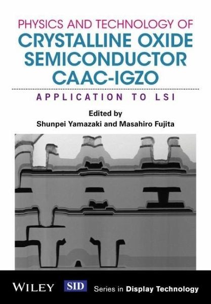
This book describes the application of c-axis aligned crystalline In-Ga-Zn oxide (CAAC-IGZO) technology in large-scale integration (LSI) circuits. The applications include Non-volatile Oxide Semiconductor Random Access Memory (NOSRAM), Dynamic Oxide Semiconductor Random Access Memory (DOSRAM), central processing unit (CPU), field-programmable gate array (FPGA), image sensors, and etc. The book also covers the device physics (e.g., off-state characteristics) of the CAAC-IGZO field effect transistors (FETs) and process technology for a hybrid structure of CAAC-IGZO and Si FETs. It explains an…mehr
This book describes the application of c-axis aligned crystalline In-Ga-Zn oxide (CAAC-IGZO) technology in large-scale integration (LSI) circuits. The applications include Non-volatile Oxide Semiconductor Random Access Memory (NOSRAM), Dynamic Oxide Semiconductor Random Access Memory (DOSRAM), central processing unit (CPU), field-programmable gate array (FPGA), image sensors, and etc. The book also covers the device physics (e.g., off-state characteristics) of the CAAC-IGZO field effect transistors (FETs) and process technology for a hybrid structure of CAAC-IGZO and Si FETs. It explains an extremely low off-state current technology utilized in the LSI circuits, demonstrating reduced power consumption in LSI prototypes fabricated by the hybrid process. A further two books in the series will describe the fundamentals; and the specific application of CAAC-IGZO to LCD and OLED displays.
Key features:
_ Outlines the physics and characteristics of CAAC-IGZO FETs that contribute to favorable operations of LSI devices. _ Explains the application of CAAC-IGZO to LSI devices, highlighting attributes including low off-state current, low power consumption, and excellent charge retention. _ Describes the NOSRAM, DOSRAM, CPU, FPGA, image sensors, and etc., referring to prototype chips fabricated by a hybrid process of CAAC-IGZO and Si FETs.Hinweis: Dieser Artikel kann nur an eine deutsche Lieferadresse ausgeliefert werden.
Shunpei Yamazaki, Semiconductor Energy Laboratory Co., Ltd., Kanagawa, JAPAN Dr. Shunpei Yamazaki is an authority on semiconductors, memory devices, and liquid crystal displays. Listed on over 4,000 US utility patents, Dr. Yamazaki was named in the Guinness Book of World Records as holding the most patents in the world; hailed the most prolific inventor in history by USA Today (in 2005). His most notable work is on the thin-film transistor -- a significant discovery being a crystalline structure in Indium gallium zinc oxide (IGZO) material, which he discovered "by chance" in 2009. Today Dr. Yamazaki is President of the Semiconductor Energy Laboratory (SEL), where he and his team pioneered the unique development of ultra-low-power devices using CAAC-IGZO technology. A joint venture with the Sharp Corporation manufacturing smartphones using crystalline oxide semiconductors (IGZO) is a global first. In 2015 Dr. Yamazaki received the SID (Society for Information Display) Special Recognition Award for "discovering CAAC-IGZO semiconductors, leading its practical application, and paving the way to next-generation displays." His paper on CAAC-IGZO ranked in the top 15 most downloaded papers of Wiley Electrical Engineering and Communications Technology journals, 2014. Dr. Yamazaki is also an IEEE Life Fellow. Masahiro Fujita, University of Tokyo, Japan Masahiro Fujita: received his Ph.D. in Information Engineering from the University of Tokyo in 1985 on his work on model checking of hardware designs by using logic programming languages. In 1985, he joined Fujitsu as a researcher and started to work on hardware automatic synthesis as well as formal verification methods and tools. From 1993 to 2000, he was director at Fujitsu Laboratories of America and headed a hardware formal verification group developing a formal verifier for real-life designs. Since March 2000, he has been a professor at VLSI Design and Education Center of the University of Tokyo. He has authored and co-authored more than 10 books and 300 publications, and has been given several awards from scientific societies. His research interests include synthesis and verification of hardware and software systems.
Inhaltsangabe
About the Editors x
List of Contributors xii
Series Editor's Foreword xiii
Preface xv
Acknowledgments xviii
1 Introduction 1
1.1 Overview of this Book 1
1.2 Background 3
1.2.1 Typical Characteristics of CAAC-IGZO FETs 3
1.2.2 Possible Applications of CAAC-IGZO FETs 4
1.3 Summary of Each Chapter 7
References 9
2 Device Physics of CAAC-IGZO FET 11
2.1 Introduction 11
2.2 Off-State Current 14
2.2.1 Off-State Current Comparison between Si and CAAC-IGZO FETs 14
2.2.2 Measurement of Extremely Low Off-State Current 16
2.2.3 Theoretical Discussion with Energy Band Diagram 23
2.2.4 Conclusion 28
2.3 Subthreshold Characteristics 29
2.3.1 Estimation of Icut by SS 30
2.3.2 Extraction Method of Interface Levels 33
2.3.3 Reproduction of Measured Value and Estimation of Icut 35
2.3.4 Conclusion 38
2.4 Technique for Controlling Threshold Voltage (Vth) 39
2.4.1 Vth Control by Application of Back-Gate Bias 39
2.4.2 Vth Control by Formation of Circuit for Retaining Back-Gate Bias 42
2.4.3 Vth Control by Charge Injection into the Charge Trap Layer 45
2.4.4 Conclusion 49
2.5 On-State Characteristics 49
2.5.1 Channel-Length Dependence of Field-Effect Mobility 50
2.5.2 Measurement of Cut-off Frequency 59
2.5.3 Summary 62
2.6 Short-Channel Effect 62
2.6.1 Features of S-ch CAAC-IGZO FETs 63
2.6.2 Effect of S-ch Structure 70
2.6.3 Intrinsic Accumulation-Mode Device 71
2.6.4 Dielectric Anisotropy 74
2.6.5 Numerical Calculation of the Band Diagrams in IGZO FETs 76
2.6.6 Summary 82
2.7 20-nm-Node CAAC-IGZO FET 83
2.7.1 TGSA CAAC-IGZO FET 83
2.7.2 Device Characteristics 86
2.7.3 Memory-Retention Characteristics 89
2.7.4 Summary 92
2.8 Hybrid Structure 92
2.8.1 TGTC Structure 93
2.8.2 TGSA Structure 94
2.8.3 Hybrid Structure 96
Appendix: Comparison between CAAC-IGZO and Si 98
References 99
3 NOSRAM 102
3.1 Introduction 102
3.2 Memory Characteristics 103
3.3 Application of CAAC-IGZO FETs to Memory and their Operation 104
3.4 Configuration and Operation of NOSRAM Module 106
3.4.1 NOSRAM Module 106
3.4.2 Setting Operational Voltage of NOSRAM Module 106
3.4.3 Operation of NOSRAM Module 108
3.5 Multilevel NOSRAM 108
3.5.1 4-Level (2 Bits/Cell) NOSRAM Module 110
3.5.2 8-Level (3 Bits/Cell) NOSRAM Module 112
3.5.3 16-Level (4 Bits/Cell) NOSRAM Module 114
3.5.4 Stacked Multilevel NOSRAM 119
3.6 Prototype and Characterization 120
3.6.1 2-Level NOSRAM 120
3.6.2 4-Level NOSRAM 128
3.6.3 8-Level NOSRAM 128
3.6.4 16-Level NOSRAM 129
3.6.5 Comparison of Prototypes 133
References 136
4 DOSRAM 137
4.1 Introduction 137
4.2 Characteristics and Problems of DRAM 138
4.3 Operations and Characteristics of DOSRAM Memory Cell 138
4.4 Configuration and Basic Operation of DOSRAM 139
4.4.1 Circuit Configuration and Operation of DOSRAM 139