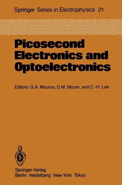
Picosecond Electronics and Optoelectronics
Proceedings of the Topical Meeting Lake Tahoe, Nevada, March 13-15, 1985
Herausgegeben von Mourou, Gerard A.; Bloom, David M.; Lee, Chi-H.
Versandkostenfrei!
Versandfertig in 1-2 Wochen
123,99 €
inkl. MwSt.

PAYBACK Punkte
62 °P sammeln!
Over the past decade, we have witnessed a number of spectacular advances in the fabrication of crystalline semiconductor devices due mainly to the pro gress of the different techni ques of heteroepitaxy. The di scovery of two dimensional behavior of electrons led to the development of a new breed of ultrafast electronic and optical devices, such as modulation doped FETs, permeable base transistors, and double heterojunction transistors. Comparable progress has been made in the domain of cryoelectronics, ultrashort pulse generation, and ultrafast diagnostics. Dye lasers can generate 8 fs signal...
Over the past decade, we have witnessed a number of spectacular advances in the fabrication of crystalline semiconductor devices due mainly to the pro gress of the different techni ques of heteroepitaxy. The di scovery of two dimensional behavior of electrons led to the development of a new breed of ultrafast electronic and optical devices, such as modulation doped FETs, permeable base transistors, and double heterojunction transistors. Comparable progress has been made in the domain of cryoelectronics, ultrashort pulse generation, and ultrafast diagnostics. Dye lasers can generate 8 fs signals after compression, diode lasers can be modulated at speeds close to 20 GHz and electrical signals are characterized with subpicosecond accuracy via the electro-optic effect. Presently, we are experiencing an important interplay between the field of optics and electronics; the purpose of this meeting was to foster and enhance the interaction between the two disciplines. It was logical to start the conference by presenting to the two different audiences, i. e. , electronics and optics, the state-of-the-art in the two res pective fields and to highlight the importance of optical techniques in the analysis of physical processes and device performances. One of the leading techniques in this area is the electro-optic sampling technique. This optical technique has been used to characterize transmission lines and GaAs devices. Carrier transport in semiconductors is of fundamental importance and some of its important aspects are stressed in these proceedings.


