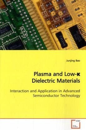
Plasma and Low- Dielectric Materials
Interaction and Application in Advanced Semiconductor Technology
Versandkostenfrei!
Versandfertig in 6-10 Tagen
52,99 €
inkl. MwSt.

PAYBACK Punkte
26 °P sammeln!
With the scaling of devices, integration of porous ultra low-k materials into Cu interconnect becomes imperative. Low-k dielectric materials consist of methyl groups and pores incorporated into a silicon dioxide backbone structure to reduce the dielectric constant. Plasma is widely used in semiconductor industry for deposition, etching, stripping etc. This book explores the interaction between plasma and low-k dielectric materials and their application in advanced semiconductor processes. It mainly consists of two parts. First, plasma assists the atomic layer deposition of Ta based Cu barriers...
With the scaling of devices, integration of porous
ultra low-k materials into Cu interconnect becomes
imperative. Low-k dielectric materials consist of
methyl groups and pores incorporated into a silicon
dioxide backbone structure to reduce the dielectric
constant. Plasma is widely used in semiconductor
industry for deposition, etching, stripping etc.
This book explores the interaction between plasma
and low-k dielectric materials and their application
in advanced semiconductor processes. It mainly
consists of two parts. First, plasma assists the
atomic layer deposition of Ta based Cu barriers.
Experiments, coupled with Monte Carlo simulation
proved that plasma alters low-k surfaces and
generates favorable surface function groups for
subsequent Ta/TaN deposition. Second, plasma
degrades properties of low-k materials through
methyl depletion. Mechanism of plasma damage to
blanket and pattern low-k films was discussed. Then
techniques for low-k repair, such as methane beam
and silylation, were demonstrated.


