Plasma Ashing
Versandkostenfrei!
Versandfertig in 6-10 Tagen
32,99 €
inkl. MwSt.

PAYBACK Punkte
16 °P sammeln!
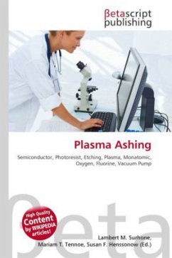
Please note that the content of this book primarily consists of articles available from Wikipedia or other free sources online. In semiconductor manufacturing plasma ashing is the process of removing the photoresist from an etched wafer. Using a plasma source, a monatomic reactive species is generated. Oxygen or fluorine are the most common reactive species. The reactive species combines with the photoresist to form ash which is removed with a vacuum pump.Typically, monatomic (single atom) oxygen plasma is created by exposing oxygen gas (O2) to non-ionizing radiation. This process is done unde...
Please note that the content of this book primarily consists of articles available from Wikipedia or other free sources online. In semiconductor manufacturing plasma ashing is the process of removing the photoresist from an etched wafer. Using a plasma source, a monatomic reactive species is generated. Oxygen or fluorine are the most common reactive species. The reactive species combines with the photoresist to form ash which is removed with a vacuum pump.Typically, monatomic (single atom) oxygen plasma is created by exposing oxygen gas (O2) to non-ionizing radiation. This process is done under vacuum in order to create a plasma. As the plasma is formed, many free radicals are created which could damage the wafer. Newer, smaller circuitry is increasingly susceptible to these particles.


