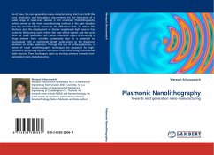
Plasmonic Nanolithography
Towards next generation nano-manufacturing
Versandkostenfrei!
Versandfertig in 6-10 Tagen
39,99 €
inkl. MwSt.

PAYBACK Punkte
20 °P sammeln!
As of now, the next-generation nano-manufacturing which can fulfill the cost, resolution, and throughput requirements for the fabrication of a wide range of nano-scale devices is still uncertain. Photolithography which served as the main manufacturing method in the past decades has the resolution limit, known as the diffraction limit. To reduce the features size, the employment of shorter wavelength light sources has come to the turning point where the cost of the system and the cycle time for mask fabrication are critical. Plasmonic optics is attracting a huge interest from scientific communi...
As of now, the next-generation nano-manufacturing which can fulfill the cost, resolution, and throughput requirements for the fabrication of a wide range of nano-scale devices is still uncertain. Photolithography which served as the main manufacturing method in the past decades has the resolution limit, known as the diffraction limit. To reduce the features size, the employment of shorter wavelength light sources has come to the turning point where the cost of the system and the cycle time for mask fabrication are critical. Plasmonic optics is attracting a huge interest from scientific community due to a potential to manipulate light at nanometer length scale owing to the dispersive behavior of surface plasmons. Through the use of surface plasmons, a series of novel nanolithography techniques are proposed for high-resolution patterning beyond diffraction limit while using conventional light sources. These techniques open up exciting avenues towards next-generation nano-manufacturing.


