Jetzt bewerten Jetzt bewerten
An authoritative single-volume reference on the design and analysis of ESD protection for ICs Electrostatic discharge (ESD) is a major reliability challenge to semiconductors, integrated circuits (ICs), and microelectronic systems. On-chip ESD protection is a vital to any electronic products, such as smartphones, laptops, tablets, and other electronic devices. Practical ESD Protection Design provides comprehensive and systematic guidance on all major aspects of designs of on-chip ESD protection for integrated circuits (ICs). Written for students and practicing engineers alike, this one-stop …mehr
Andere Kunden interessierten sich auch für
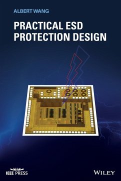
An authoritative single-volume reference on the design and analysis of ESD protection for ICs Electrostatic discharge (ESD) is a major reliability challenge to semiconductors, integrated circuits (ICs), and microelectronic systems. On-chip ESD protection is a vital to any electronic products, such as smartphones, laptops, tablets, and other electronic devices. Practical ESD Protection Design provides comprehensive and systematic guidance on all major aspects of designs of on-chip ESD protection for integrated circuits (ICs). Written for students and practicing engineers alike, this one-stop resource covers essential theories, hands-on design skills, computer-aided design (CAD) methods, characterization and analysis techniques, and more on ESD protection designs. Detailed chapters examine an array of topics ranging from fundamental to advanced, including ESD phenomena, ESD failure analysis, ESD testing models, ESD protection devices and circuits, ESD design layout and technology effects, ESD design flows and co-design methods, ESD modelling and CAD techniques, and future ESD protection concepts. Based on the author's decades of design, research and teaching experiences, Practical ESD Protection Design - Features numerous real-world ESD protection design examples - Emphasizes on ESD protection design techniques and procedures - Describes ESD-IC co-design methodology for high-performance mixed-signal ICs and broadband radio-frequency (RF) ICs - Discusses CAD-based ESD protection design optimization and prediction using both Technology and Electrical Computer-Aided Design (TCAD/ECAD) simulation - Addresses new ESD CAD algorithms and tools for full-chip ESD physical design verification - Explores the disruptive future outlook of ESD protection Practical ESD Protection Design is a valuable reference for industrial engineers and academic researchers in the field, and an excellent textbook for electronic engineering courses in semiconductor microelectronics and integrated circuit designs.
Hinweis: Dieser Artikel kann nur an eine deutsche Lieferadresse ausgeliefert werden.
Produktdetails
Verlag: Wiley Seitenzahl: 432 Erscheinungstermin: 6. Januar 2022 Englisch Abmessung: 260mm x 183mm x 28mm Gewicht: 1005g ISBN-13: 9781119850403 ISBN-10: 1119850401 Artikelnr.: 62117397
Albert Wang, PhD, is a Professor in the Department of Electrical and Computer Engineering at the University of California, Riverside, USA. He was an IC designer in the Silicon Valley before joining the academia. His research resulted in two books, more than 300 peer-reviewed papers, and 16 granted U.S. patents. He was the President of IEEE Electron Devices Society. He is a Fellow of the National Academy of Inventors and a Fellow of IEEE.
Author Biography xi Preface xiii 1 Why ESD? 1 1.1 A Historical Perspective 1 1.2 ESD and the Dangers 3 1.3 ESD Protection: The Principles 9 1.4 ESD Protection: More or Less? 13 1.5 ESD Protection: Evolution to Revolution 15 References 15 2 ESD Failure Analysis 19 2.1 ESD Failure Analysis 19 2.1.1 ESD Failure Criteria 19 2.1.2 Hard and Soft ESD Failures 20 2.2 ESD FA Techniques 20 2.3 ESD Failure Signatures 22 2.4 ESD Soft Failures 38 2.5 ESD Failure Correlation 41 2.6 ESD Failure Models 44 References 47 3 ESD Test Models and Standards 51 3.1 ESD Origins 51 3.2 HBM Model 52 3.3 mm Model 58 3.4 CDM Model 61 3.5 IEC Model 67 3.6 TLP Model 69 3.7 Summary 74 References 75 4 ESD Protection Devices 77 4.1 On-Chip ESD Protection Mechanisms 77 4.1.1 Switch for ESD Discharge 77 4.1.2 ESD Protection: Active versus Passive 81 4.2 Diode for ESD Protection 84 4.2.1 Diode Device Physics 84 4.2.2 Diode in ESD Protection 85 4.2.3 Diode ESD Parasitic Modeling 87 4.3 BJT for ESD Protection 87 4.3.1 BJT Device Physics 88 4.3.2 BJT in ESD Protection 90 4.3.3 BJT ESD Parasitic Modeling 92 4.4 MOSFET for ESD Protection 93 4.4.1 MOSFET Device Physics 94 4.4.2 ggMOS in ESD Protection 95 4.4.3 MOSFET ESD Parasitic Modeling 98 4.5 SCR for ESD Protection 99 4.5.1 SCR Device Physics 100 4.5.2 SCR in ESD Protection 102 4.5.3 SCR ESD Parasitic Modeling 106 4.6 Summary 107 References 109 5 ESD Protection Circuits 111 5.1 I/O ESD Protection 111 5.1.1 Two-Stage ESD Protection 112 5.1.2 Multiple-Fingers ESD Protection 113 5.1.3 MOSFET ESD Protection Circuits 114 5.1.4 BJT ESD Protection Circuits 117 5.1.5 SCR ESD Protection Circuits 120 5.2 ESD Self-Protection 121 5.2.1 Output ESD Protection 121 5.2.2 ESD Self-Protection 124 5.3 Low-Triggering ESD Protection Circuits 124 5.4 ESD Power Clamps 129 5.4.1 Diode-String Power Clamps 131 5.4.2 MOSFET Power Clamps 134 5.4.3 SCR Power Clamps 135 5.4.4 Any Switch Power Clamps 135 5.5 Summary 136 References 137 6 Full-Chip ESD Protection 139 6.1 Full-Chip ESD Protection Principles 139 6.2 ESD Protection Design Window 140 6.3 Advanced ESD Protection: More at Less 142 6.3.1 Dual-Polarity ESD Protection 143 6.3.2 Multiple-Polarity ESD Protection 147 6.4 Full-Chip ESD Protection Schemes 150 6.4.1 Full-Chip ESD Consideration 150 6.4.2 Pad-Clamp Scheme 151 6.4.3 Global ESD Bus Scheme 153 6.5 No Universal ESD Protection Solution 154 References 155 7 Mixed-Signal and HV ESD Protection 157 7.1 ESD Protection for Mixed-Signal ICs 157 7.2 ESD Protection for Multiple-Voltages ICs 162 7.3 ESD Protection for High-Voltage ICs 167 7.3.1 ESD Design Window Compliance 167 7.3.2 Latch-up Immunity 173 7.4 Summary 174 References 175 8 TCAD-Based Mixed-Mode ESD Protection Designs 177 8.1 ESD Design Optimization and Prediction 177 8.2 TCAD-Based Mixed-Mode ESD Simulation-Design Methodology 182 8.3 Mixed-Mode ESD Simulation-Design Examples 188 8.3.1 Example 1: Understand TCAD ESD Simulation 188 8.3.2 Example-2: ggNMOS versus gcNMOS ESD Protection 192 8.3.3 Example-3: ESD Power Clamp in 0.35 ¿mCMOS 196 8.3.4 Example-4: Optimize HV ESD Protection Design 199 8.3.5 Example-5: ESD Layout Analysis by 3D TCAD 203 8.3.6 Example-6: Multiple-Stimuli TCAD ESD Simulation 210 8.4 Summary 218 References 219 9 RF ESD Protection 221 9.1 What Is Special for RF ESD Protection? 221 9.2 RF ESD Protection Characterization 226 9.3 Low-Parasitic ESD Protection Solutions 232 9.4 RF ESD Protection Design Example 233 9.5 Summary 236 References 237 10 ESD-RFIC Co-Design 239 10.1 ESD-IC Interactions 239 10.1.1 IC Affects ESD Protection 239 10.1.2 ESD Affects IC Performance 241 10.2 ESD-RFIC Co-Design 248 10.2.1 ESD-RFIC Co-Design Principle 249 10.2.2 ESD-RFIC Co-Design Examples 251 10.3 Summary 259 References 259 11 ESD Layout Designs 261 11.1 Layout is Critical to ESD Protection 261 11.2 Basic ESD Protection Layout 262 11.3 Advanced ESD Protection Layout 274 11.3.1 Advanced ESD Layout Considerations 274 11.3.2 ESD Design Layout is an Art 278 11.4 3D TCAD for ESD Layout Designs 284 11.5 Summary 294 References 295 12 ESD versus IC Technologies 297 12.1 IC Technologies and ESD Protection 297 12.1.1 ESD Metal Interconnects 297 12.1.2 Technology-ESD Co-Development 299 12.1.3 Graphene Heat Spreading 305 12.2 Technology Affects ESD Design Window 305 12.3 Lowering ESD Protection for Advanced ICs? 306 12.4 Summary 308 References 308 13 ESD Circuit Simulation by SPICE 311 13.1 ESD Device Behavior Modeling 311 13.2 Full-Chip ESD Circuit Simulation by SPICE 314 13.2.1 Principle for ESD Circuit Simulation by SPICE 314 13.2.2 Circuit-Level ESD Design Verification by SPICE 319 13.3 Summary 326 References 326 14 Emerging ESD Protection 327 14.1 Emerging ESD Protection Challenges 327 14.2 Dispensable ESD Protection 328 14.3 Field-Programmable ESD Protection 332 14.3.1 Nano-Crystal Quantum-Dots ESD Protection 332 14.3.2 SONOS ESD Protection 334 14.4 Interposer/TSV-Based ESD Protection 337 14.5 Summary 341 References 342 15 ESD CAD for Full-Chip Design Verification 345 15.1 Full-Chip ESD Design Verification 345 15.2 CAD Algorithms for ESD Design Verification 347 15.3 Full-Chip ESD Design Verification Examples 353 15.4 Summary 363 References 364 16 New CDM ESD Protection 367 16.1 Misconception in CDM ESD Protection 367 16.2 Analyzing Pad-Based CDM ESD Protection 370 16.3 Internally Distributed CDM ESD Protection 385 16.4 Summary 391 References 392 17 Future ESD Protection Outlook 395 17.1 The Fundamental ESD Protection Problem 395 17.2 Above-IC Nano-Crossbar Array ESD Switch 396 17.3 Graphene ESD Protection Switch 401 17.4 Graphene ESD Protection Interconnects 405 17.5 Future ESD Protection Outlook 407 17.6 Summary 410 References 411 Index 413