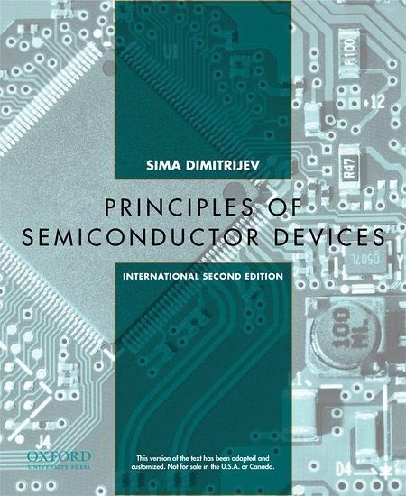
Sima Dimitrijev (, Professor, School of Microelectronic Engineering
Principles of Semiconductor Devices
International Second Edition
Sima Dimitrijev (, Professor, School of Microelectronic Engineering
Principles of Semiconductor Devices
International Second Edition
- Broschiertes Buch
- Merkliste
- Auf die Merkliste
- Bewerten Bewerten
- Teilen
- Produkt teilen
- Produkterinnerung
- Produkterinnerung
For the international second edition, the author builds upon and expands on hallmark features of the book established in the first edition, adding sections on new technology and increasing the number of end-of-chapter problems by 30%. Updated material relating to the environmental applications of technology was added , as well as a new chapter on nanoscale devices. Chapters on MOS capacitor and generation and recombination were also revised and updated.
Andere Kunden interessierten sich auch für
- M. S. Tyagi (Indian Institute of Technology, Kanpur, India)Introduction to Semiconductor Materials and Devices262,99 €
- Reliability of Semiconductor Lasers and Optoelectronic Devices171,99 €
- Handbook of GaN Semiconductor Materials and Devices57,99 €
- Simon M. Sze (Inc. Bell Laboratories)Semiconductor Devices341,99 €
- Debdeep Jena (Professor of Electrical and Computer Engineering andQuantum Physics of Semiconductor Materials and Devices149,99 €
- KASAPPrinciples of Electronic Materials and Devices81,99 €
- Adrian Kitai (McMaster University, Ontario, Canada)Fundamentals of Semiconductor Materials and Devices117,99 €
-
-
-
For the international second edition, the author builds upon and expands on hallmark features of the book established in the first edition, adding sections on new technology and increasing the number of end-of-chapter problems by 30%. Updated material relating to the environmental applications of technology was added , as well as a new chapter on nanoscale devices. Chapters on MOS capacitor and generation and recombination were also revised and updated.
Hinweis: Dieser Artikel kann nur an eine deutsche Lieferadresse ausgeliefert werden.
Produktdetails
- Produktdetails
- The Oxford Series in Electrical and Computer Engineering
- Verlag: Oxford University Press Inc
- 2 Revised edition
- Seitenzahl: 576
- Erscheinungstermin: 5. Januar 2012
- Englisch
- Abmessung: 231mm x 188mm x 27mm
- Gewicht: 962g
- ISBN-13: 9780199896349
- ISBN-10: 0199896348
- Artikelnr.: 47867081
Sima Dimitrijev is Professor at the School of Microelectronic Engineering at Griffith University in Australia. He is the author of Understanding Semiconductor Devices (OUP, 2000) as well as numerous other publications in the areas of MOSFET technology, modeling and applications.
* PART I INTRODUCTION TO SEMICONDUCTORS
* 1 lNTRODUCTION TO CRYSTALS AND CURRENT CARRIERS
* IN SEMICONDUCTORS, THE ATOMIC-BOND MODEL
* 1.1 INTRODUCTION TO CRYSTALS
* 1.1.1 Atomic Bonds
* 1.1.2 Three-Dimensional Crystals
* 1.1.3 Two-Dimensional Crystals: Graphene and Carbon Nanotubes
* 1.2 CURRENT CARRIERS
* 1.2.1 Two Types of Current Carriers in Semiconductors
* 1.2.2 N·Type and P-Type Doping
* 1.2.3 Electroneutrality Equation
* 1.2.4 Electron and Hole Generation and Recombination in Thermal
Equilibrium
* 1.3 BASICS OF CRYSTAL GROWTH AND DOPING TECHNIQUES
* 1.3.1 Crystal-Growth Techniques
* 1.3.2 Doping Techniques
* Summary
* Problems
* Review Questions
* 2 THE ENERGY-BAND MODEL
* 12.1 ELECTRONS AS WAVES
* 2.1.1 De Broglie Relationship Between Particle and Wave Properties
* 2.1.2 Wave Function and Wave Packet
* 2.1.3 Schrodinger Equation
* 2.2 ENERGY LEVELS IN ATOMS AND ENERGY BANDS IN CRYSTALS
* 2.2.1 Atomic Structure
* 2.2.2 Energy Bands in Metals
* 2.2.3 Energy Gap and Energy Bands in Semiconductors and Insulators
* 12.3 ELECTRONS AND HOLES AS PARTICLES
* 2.3.1 Effective Mass and Real E-k Diagrams
* 2.3.2 The Question of Electron Size: The Uncertainty Principle
* 2.3.3 Density of Electron States
* 2.4 POPULATION OF ELECTRON STATES, CONCENTRATIONS OF
* ELECTRONS A:"D HOLES
* 2.4.1 Fermi-Dirac Distribution
* 2.4.2 Maxwell-Boltzmann Approximation and Effective Density of States
* 2.4.3 Fermi Potential and Doping
* 2.4.4 Nonequilibrium Carrier Concentrations and Quasi-Fermi Levels
* Summary
* Problems
* Review Questions
* 3 DRIFT
* 3.1 ENERGY BANDS WITH APPLIED ELECTRIC FIELD
* 3.1.1 Energy-Band Presentation of Drift Current
* 3.1.2 Resistance and Power Dissipation due to Carrier Scattering
* 3.2 OHM'S LAW, SHEET RESISTANCE, AND CONDUCTIVITY
* 3.2.1 Designing Integrated-Circuit Resistors
* 3.2.2 Differential Form of Ohm's Law
* 3.2.3 Conductivity Ingredients
* 3.3 CARRIER MOBILITY
* 3.3.1 Thermal and Drift Velocities
* 3.3.2 Mobility Definition
* 3.3.3 Scattering Time and Scattering Cross Section
* 3.3.4 Mathieson's Rule
* °3.3.5 Hall Effect
* Summary
* Problems
* Review Questions
* 4 DlFFUSION
* 4.1 DIFFUSION-CURRENT EQUATION
* 4.2 DIFFUSION COEFFICIENT
* 4.2.1 Einstein Relationship
* L4.2.2 Haynes-Shockley Experiment
* 4.2.3 Arrhenius Equation
* 4.3 BASIC CONTINUITY EQUATION
* Summary
* Problems
* Review Questions
* 5 GENERATION AND RECOMBINATION
* 5.1 GENERATION AND RECOMBINATION MECHANISMS
* 5.2 GENERAL FORM OF THE CONTINUITY EQUATION
* 5.2.1 Recombination and Generation Rates
* 5.2.2 Minority-Carrier Lifetime
* 5.2.3 Diffusion Length
* 5.3 GENERATION AND RECOMBINATION PHYSICS AND SHOCKLEYREAD-
* HALL (SRH) THEORY
* 5.3.1 Capture and Emission Rates in Thermal Equilibrium
* 5.3.2 Steady-State Equation for the Effective Thermal
Generation/Recombination
* Rate
* 5.3.3 Special Cases
* 5.3.4 Surface Generation and Recombination
* Summary
* Problems
* Review Questions
* PART II FUNDAMENTAL DEVICE STRUCTURES
* 6 JUNCTIONS
* 6.1 P-N JUNCTION PRINCIPLES
* 6.1.1 p-~ Junction in Thermal Equilibrium
* 6.1.2 Reverse-Biased P-N Junction
* 6.1.3 Forward-Biased P-K Junction
* 6.1.4 Breakdown Phenomena
* 6.2 DC MODEL
* 6.2.1 Basic Current-Voltage (I-V) Equation
* 6.2.2 Important Second-Order Effects
* 6.2.3 Temperature Effects
* 6.3 CAPACITA CE OF REVERSE-BIASED P-:-I JUNCTION
* 6.3.1 C-V Dependence
* 6.3.2 Depletion-Layer Width: Solving the Poisson Equation
* 6.3.3 SPICE Model for the Depletion-Layer Capacitance
* 6.4 STORED-CHARGE EFFECTS
* 6.4.1 Stored Charge and Transit Time
* 6.4.2 Relationship Between the Transit Time and the Minority-Carrier
* Lifetime
* 6.4.3 Switching Characteristics: Reverse-Recovery Time
* 6.5 METAL-SEMICONDUCTOR CONTACT
* 6.5.1 Schottky Diode: Rectifying Metal-Semiconductor Contact
* 6.5.2 Ohmic Metal-Semiconductor Contacts
* Summary
* Problems
* Review Questions
* 7 MOSFET
* 7.1 MOS CAPACITOR
* 7.1.1 Properties of the Gate Oxide and the Oxide-Semiconductor
Interface
* 7.1.2 C-V Curve and the Surface-Potential Dependence on Gate Voltage
* 7.1.3 Energy-Band Diagrams
* 7.1.4 Flat4Band Capacitance and Debye Length
* 7.2 MOSFET PRINCIPLES
* B.1.1 MOSFET Structure
* 7.2.2 MOSFET as a Voltage-Controlled Switch
* B.1.3 The Threshold Voltage and the Body Effect
* B.1.4 MOSFET as a Voltage-Controlled Current Source: Mechanisms of
* Current Saturation
* 7.3 PRINCIPAL CURRENT-VOLTAGE CHARACTERISTICS AND EQUATIONS
* 7.3.1 SPICE LEVEL 1 Model
* 7.3.2 SPICE LEVEL 2 Model
* 7.3.3 SPICE LEVEL 3 Model: Principal Effects
* 7.4 SECO:\D-OROER EFFECTS
* 7.4.1 Mobility Reduction with Gate Voltage
* 7.4.2 Velocity Saturation (Mobility Reduction with Drain Voltage)
* 7.4.3 Finite Output Resistance
* 7.4.4 Threshold-Voltage-Related Short-Channel Effects
* 7.4.5 Threshold Voltage Related Narrow-Channel Effects
* 7.4.6 Subthreshold Current
* 7.5 Nanoscale MOSFETs
* 7.5.1 Down-Scaling Benefits and Rules
* 7.5.2 Leakage Currents
* 7.5.3 Advanced MOSFETs
* 7.6 MOS-BASED MEMORY DEVICES
* 7.6.1 1C1T DRAM Cell
* 7.6.2 Flash-Memory Cell
* Summary
* Problems
* Review Questions
* 8 BJT
* 8.1 B.JT PRINCIPLES
* 8.1.1 BJT as a Voltage-Controlled Current Source
* 8.1.2 BJT Currents and Gain Definitions
* 8.1.3 Dependence of ? and ? Current Gains on Technological Parameters
* 8.1.4 The Four Modes of Operation: BJT as a Switch
* 8.1.5 Complementary BJT
* 8.1.6 BJT Versus MOSFET
* 8.2 PRINCIPAL CURRENT-VOLTAGE CHARACTERISTICS, EBERE-MOLL
* MODEL IN SPICE
* 8.2.1 Injection Version
* 8.2.2 Transport Version
* 8.2.3 SPICE Version
* 8.3 SECOND·ORDER EFFECTS
* 8.3.1 Early Effect: Finite Dynamic Output Resistance
* 8.3.2 Parasitic Resistances
* 8.3.3 Dependence of Common-Emitter Current Gain on Transistor
Current:
* Low-Current Effects
* 8.3.4 Dependence of Common-Emitter Current Gain on Transistor
Current:
* Gummel-Poon Model for High-Current Effects
* 8.4 HETEROJUNCTION BIPOLAR TRANSISTOR
* Summary
* Problems
* Review Questions
* PART III SUPPLEMENTARY TOPICS
* 9 PHYSICS OF NANOSCALE DEVICES
* 9.1 SINGLE-CARRIER EVENTS
* 9.1.1 Beyond the Classical Principle of Continuity
* 9.1.2 Current-Time Form of Uncertainty Principle
* 9.1.3 Carrier-Supply Limit to Diffusion Current
* 9.1.4 Spatial Uncertainty
* 9.1.5 Direct Nonequilibrium Modeling of Single-Carrier Events
* 9.2 TWO-DIMENSIONAL TRANSPORT IN MOSFETs AND HEMTs
* 9.2.1 Quantum Confinement
* 9.2.2 HEMT Structure and Characteristics
* 9.2.3 Application of Classical MOSFET Equations to Two-Dimensional
* Transport in MOSFETs and HEMTs
* 9.3 ONE-DIMENSUIONAL TRANSPORT IN NANOWIRES AND CARBON
* NANOTUBES
* 9.3.1 Ohmic Transport in Nanowire and Carbon-Nanotube FETs
* 9.3.2 One-Dimensional Ballistic Transport and the Quantum Conductance
* Limit
* Summary
* Problems
* Review Questions
* 10 DEVICE ELECTRONICS, EQUIVALENT CIRCUITS A D SPICE
* PARAMETERS
* 10.l DIODES
* 10.1.1 Static Model and Parameters in SPICE
* 10.1.2 Large-Signal Equivalent Circuit in SPICE
* 10.1.3 Parameter Measurement
* 10.1.4 Small-Signal Equivalent Circuit
* 10.2 MOSFET
* 10.2.1 Static Model and Parameters; LEVEL 3 in SPICE
* 10.2.2 Parameter Measurement
* 10.2.3 Large-Signal Equivalent Circuit and Dynamic Parameters in
SPICE
* 10.2.4 Simple Digital ~1od.el
* 10.2.5 Small-Signal Equivalent Circuit
* 10.3 BJT
* 10.3.1 Static Model and Parameters: Ebers-Moll and Gummel-Poon Levels
* in SPICE
* 10.3.2 Parameter Measurement
* 10.3.3 Large-Signal Equivalent Circuit and Dynamic Parameters in
SPICE
* 10.3.4 Small-Signal Equivalent Circuit
* Summary
* Problems
* Review Questions
* 11 PHOTONIC DEVICES
* 11.1 LIGHT EMITTING DIODES (LED)
* 11.2 PHOTODETECTORS AND SOLAR CELLS
* 11.2.1 Biasing for Photodetector and Solar-Cell Applications
* 11.2.2 Carrier Generation in Photodetectors and Solar Cells
* 11.2.3 Photocurrent Equation
* 11.3 LASERS
* 11.3.1 Stimulated Emission, Inversion Population, and Other
Fundamental Concepts
* 11.3.2 A Typical Heterojunction Laser
* Summary
* Problems
* Review Questions
* 12 JFET AND MESFET
* 12.1 JFET
* 12.1.1 JFET Structure
* 12.1.2 JFET Characteristics
* 12.1.3 SPICE Model and Parameters
* 12.2 MESFET
* 12.2.1 MESFET Structure
* 12.2.2 MESFET Characteristics
* 12.2.3 SPICE Model and Parameters
* Summary
* Problems
* Review Questions
* 13 POWER DEVICES
* 13.1 POWER DIODES
* 13.1.1 Drift Region in Power Devices
* 13.1.2 Switching Characteristics
* 13.1.3 Schottky Diode
* 13.2 POWER MOSFET
* 13.3 IGBT
* 13.4 THYRISTOR
* Summary
* Problems
* Review Questions