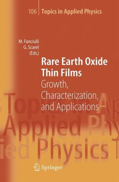
Marco Fanciulli / Giovanna Scarel (eds.)
Rare Earth Oxide Thin Films
Growth, Characterization, and Applications
Herausgegeben:Fanciulli, Marco; Scarel, Giovanna
Marco Fanciulli / Giovanna Scarel (eds.)
Rare Earth Oxide Thin Films
Growth, Characterization, and Applications
Herausgegeben:Fanciulli, Marco; Scarel, Giovanna
- Gebundenes Buch
- Merkliste
- Auf die Merkliste
- Bewerten Bewerten
- Teilen
- Produkt teilen
- Produkterinnerung
- Produkterinnerung
Thin rare earth (RE) oxide films are emerging materials for microelectronic, nanoelectronic, and spintronic applications. The state-of-the-art of thin film deposition techniques as well as the structural, physical, chemical, and electrical properties of thin RE oxide films and of their interface with semiconducting substrates are discussed. The aim is to identify proper methodologies for the development of RE oxides thin films and to evaluate their effectiveness as innovative materials in different applications.
Andere Kunden interessierten sich auch für
- Rare Earth Oxide Thin Films110,99 €
- Frontiers in Materials Research110,99 €
- K. OuraSurface Science96,29 €
- Satischandra B. OgaleThin Films and Heterostructures for Oxide Electronics184,99 €
- Thin Films and Heterostructures for Oxide Electronics110,99 €
- Roman LoubanImage Processing of Edge and Surface Defects83,99 €
- Roman LoubanImage Processing of Edge and Surface Defects74,99 €
-
-
-
Thin rare earth (RE) oxide films are emerging materials for microelectronic, nanoelectronic, and spintronic applications. The state-of-the-art of thin film deposition techniques as well as the structural, physical, chemical, and electrical properties of thin RE oxide films and of their interface with semiconducting substrates are discussed. The aim is to identify proper methodologies for the development of RE oxides thin films and to evaluate their effectiveness as innovative materials in different applications.
Produktdetails
- Produktdetails
- Topics in Applied Physics 106
- Verlag: Springer / Springer Berlin Heidelberg / Springer, Berlin
- Artikelnr. des Verlages: 11499893, 978-3-540-35796-4
- 2007
- Seitenzahl: 444
- Erscheinungstermin: 30. Oktober 2006
- Englisch
- Abmessung: 241mm x 160mm x 30mm
- Gewicht: 772g
- ISBN-13: 9783540357964
- ISBN-10: 3540357963
- Artikelnr.: 20947191
Marco Fanciulli obtained his PhD in Applied Physics from Boston University, Boston (USA) in 1993 for his work on the characterization of wide-band-gap semiconductors using magnetic resonance spectroscopies. In 1993 he joined the Institute of Physics and Astronomy at the University of Aarhus (DK) as an assistant professor to conduct research on defects in silicon using different techniques (DLTS, CEMS, EPR) and on transition metal silicides. In 1997 he was appointed associate professor. From 1998 he is the director of the MDM Laboratory. He has published more than 120 papers on the growth, by MBE, PLD, ALD, and characterization, using different spectroscopic methods most of them related to hyperfine interaction and magnetic resonance detection, of different materials. His current interests are related to the characterization of high-k materials and of the interface between semiconductors and oxides, to the development of advanced magnetic resonance characterization techniques, and to other fundamental issues related to materials and devices for microelectronics and spintronics. He coordinated the European FET assessment project ESRQC (Electron Spin Resonance for Quantum Computing) and he is the coordinator of industrial projects with STMicroelectronics. He has been the principal investigator in the EC project on nanocrystals (GROWTH: NEON - Nanoparticles for electronics) and on epitaxial high-k dielectrics (IST: INVEST- Integration of very high-k dielectrics with silicon CMOS technology) and he is currently the principal investigator on two EC projects on oxides (IST: ET4US - Epitaxial technologies for ultimate scaling; REALISE - ) as well as in other national projects. Since 2000 he is external Professor of semiconductor physics at the Department of Physics, University of Milano, Milano (Italy). Marco Fanciulli has organized and chaired several symposia (E-MRS 2001, E-MRS 2003, Euromat 2003, Silicon Workshop 2001) and a workshop on quantum computing (Germany2002). Giovanna Scarel received in June 1994 her Laurea Degree in Physics from the University of Trieste (Italy). In April 2001 Giovanna Scarel received her Ph.D from the University of Wisconsin-Milwaukee (USA). From June 2001 to February 2003 she was a post-doctoral fellow at the MDM-INFM Laboratory, where she is currently a reserach associate (tenure track position). Giovanna Scarel gained experience in surface science, where she worked on the growth and characterization of C60/Ag(110) systems and in the characterization of Al/ZnSe(001) Schottky barrier height. Giovanna Scarel was also involved in a project of normal incidence x-ray standing waves characterization of S/Rh systems at the synchrotron radiation source of Daresbury (UK). In the field of thin film growth, as a Ph.D student, Giovanna Scarel learned the reactive sputtering technique of metal oxides and used far infrared spectroscopy for the structural characterization of the films (mainly TiO2). At MDM-INFM Laboratory, she learned atomic layer deposition (ALD) of metal oxides for microelectronics. In particular, she is involved in the growth of high dielectric constant oxides relevant to substitute SiO2 in complementary metal-oxide-semiconductor (CMOS) devices. In this field, Giovanna Scarel coordinated a project at the Italian level on the ALD growth and characterization of rare earth oxides (PAIS-REOHK by INFM).
Introduction.- ALD, MOCVD, and MBE deposition of rare earth oxides. - Requirements of precursor for MOCVD and ALD of rare earth oxides.- Models for ALD and MOCVD growth of rare earth oxides.- Growth of oxides with complex stoichiometry by ALD, e.g. La1-xCaxMnO3.- Fabrication and characterization of rare earth scandate thin films prepared by pulsed laser deposition.- Film and interface layer composition of rare earth (Lu, Yb) oxides deposited by ALD.- Local atomic environment of high-k oxides on silicon probed by X-ray absorption spectroscopy, and advanced transmission electron microscopy techniques (TEM-EELS).- Strain-relief at internal dielectric interfaces in high-k gate stacks with transition metal and rare earth atom oxide dielectrics.- Electrical characterization of rare earth oxides grown by ALD.- Dielectric properties of rare-earth oxides: general trends from theory.- Charge traps in high-k dielectrics: ab initio study of defects in Pr-based materials.- Experimental determination of the band offset of rare earth oxides on various semiconductors.- Band edge electronic structure, and band offsets of transition metal/rare earth oxide dielectrics.- Rare earth oxides in microelectronics.- Requirements of oxides as gate dielectrics for CMOS devices, and ultimate scaling.- The magneto-electric properties of RMnO compounds.- Sesquioxides as host materials for rare-earth-doped bulk lasers and active waveguides.