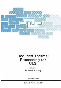
As feature dimensions of integrated circuits shrink, the associated geometrical constraints on junction depth impose severe restrictions on the thermal budget for processing such devices. Furthermore, due to the relatively low melting point of the first aluminum metallization level, such restrictions extend to the fabrication of multilevel structures that are now essential in increasing packing density of interconnect lines. The fabrication of ultra large scale integrated (ULSI) devices under thermal budget restrictions requires the reassessment of existing and the development of new…mehr
As feature dimensions of integrated circuits shrink, the associated geometrical constraints on junction depth impose severe restrictions on the thermal budget for processing such devices. Furthermore, due to the relatively low melting point of the first aluminum metallization level, such restrictions extend to the fabrication of multilevel structures that are now essential in increasing packing density of interconnect lines. The fabrication of ultra large scale integrated (ULSI) devices under thermal budget restrictions requires the reassessment of existing and the development of new microelectronic materials and processes. This book addresses three broad but interrelated areas. The first area focuses on the subject of rapid thermal processing (RTP), a technology that allows minimization of processing time while relaxing the constraints on high temperature. Initially developed to limit dopant redistribution, current applications of RTP are shown here to encompass annealing, oxidation, nitridation, silicidation, glass reflow, and contact sintering. In a second but complementary area, advances in equipment design and performance of rapid thermal processing equipment are presented in conjunction with associated issues of temperature measurement and control. Defect mechanisms are assessed together with the resulting properties of rapidly deposited and processed films. The concept of RTP integration for a full CMOS device process is also examined together with its impact on device characteristics.Hinweis: Dieser Artikel kann nur an eine deutsche Lieferadresse ausgeliefert werden.
Rapid Thermal Processing with Reactive Gases.- Rapid Thermal Processing.- Kinetics of Silicon Dielectrics by RTP.- Applications.- Polysilicon Dielectrics.- Rapid Thermal CVD: In-Situ Device Fabrication.- Summary.- Silicidation by Rapid Thermal Processing.- Reactions in the Salicide Process.- Technological Implementation.- Device Implementation of TiSi2 and CoSi2.- Conclusions.- Microstructural Defects in Rapid Thermally Processed IC Materials.- Microstructural Defects in Implanted and Subsequently Rapid Thermally Annealed Silicon Wafers.- Shallow Emitters (for Bipolar Transistors) from Doped Polysilicon Contacts.- Rapid Thermal Oxidation (RTO).- Rapid Thermal Processing of Silicides.- Concluding Remarks.- Rapid Thermal Annealing - Theory and Practice.- Transfer of Energy in Radiant Heating Systems.- Physics of Rapid Thermal Annealers Using Lamp Sources.- Modelling of Rapid Thermal Annealing - Temperature Control.- Modelling of Rapid Thermal Annealing - Temperature Uniformity.- Temperature Measurement.- Emissivity Measurement.- Temperature Non-Uniformity.- Problems and Solutions.- Practical Machine Designs.- Rapid Thermal Process Integration.- CMOS Device Processing.- Device/Circuit Operation Considerations.- Process Interaction Problems.- Process Integration Opportunities with RTP.- Summary.- to Direct Writing of Integrated Circuit.- Laser Pantography Procedure.- Resolution in Laser Pantography.- Laser Induced Temperature.- Laser Wavelength and Laser Power.- Main Difficulties in Laser Direct Writing.- Deposition and Etching Rates.- Process for Silicon Microelectronics.- Laser Induced Chemical Reactions.- Conclusion.- Ion Beam Assisted Processes.- Defect and Collision Cascade.- Ion Beam Assisted Epitaxy Regrowth.- High Current Implant.- Conclusions.-Micrometallization Technologies.- Metallization Techniques.- Ohmic Contacts.- Gate Contacts.- Barrier Layers.- Interconnections.- Multilevel Interconnect Structures.- Metal Conductor Generation.- Intermetal Insulation and Step Coverage.- Topographical Effects.- Possible Solutions to Multilevel Interconnect Problems.- Speculation on Future Multilevel Interconnect.- Interlevel Dielectrics for Reduced Thermal Processing.- Pre-Metal Planarization Process.- Requirements.- Deposition Process.- Optimization of the Flow Step.- Film Analysis.- Other Methods Involving Oxides.- Multilevel-Metal (MLM) Concepts.- Deposited Layers for MLM.- Planarization Concepts.- Depositions Incorporating In-Situ Etchback.- Conclusion.- Low Temperature Silicon Epitaxy for Novel Device Structures.- Low Temperature Epitaxy.- Auto doping, Transition Width and Dopant Incorporation/Reincorporation.- Buried Layer Pattern Transmittance.- Selective Epitaxial Growth.- Conclusion.- Participants.
Es gelten unsere Allgemeinen Geschäftsbedingungen: www.buecher.de/agb
Impressum
www.buecher.de ist ein Internetauftritt der buecher.de internetstores GmbH
Geschäftsführung: Monica Sawhney | Roland Kölbl | Günter Hilger
Sitz der Gesellschaft: Batheyer Straße 115 - 117, 58099 Hagen
Postanschrift: Bürgermeister-Wegele-Str. 12, 86167 Augsburg
Amtsgericht Hagen HRB 13257
Steuernummer: 321/5800/1497
USt-IdNr: DE450055826