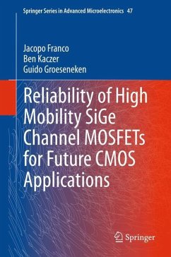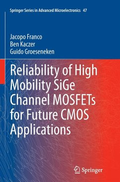
Reliability of High Mobility SiGe Channel MOSFETs for Future CMOS Applications
Versandkostenfrei!
Versandfertig in 6-10 Tagen
76,99 €
inkl. MwSt.
Weitere Ausgaben:

PAYBACK Punkte
38 °P sammeln!
Due to the ever increasing electric fields in scaled CMOS devices, reliability is becoming a showstopper for further scaled technology nodes. Although several groups have already demonstrated functional Si channel devices with aggressively scaled Equivalent Oxide Thickness (EOT) down to 5Å, a 10 year reliable device operation cannot be guaranteed anymore due to severe Negative Bias Temperature Instability.This book focuses on the reliability of the novel (Si)Ge channel quantum well pMOSFET technology. This technology is being considered for possible implementation in next CMOS technology node...
Due to the ever increasing electric fields in scaled CMOS devices, reliability is becoming a showstopper for further scaled technology nodes. Although several groups have already demonstrated functional Si channel devices with aggressively scaled Equivalent Oxide Thickness (EOT) down to 5Å, a 10 year reliable device operation cannot be guaranteed anymore due to severe Negative Bias Temperature Instability.
This book focuses on the reliability of the novel (Si)Ge channel quantum well pMOSFET technology. This technology is being considered for possible implementation in next CMOS technology nodes, thanks to its benefit in terms of carrier mobility and device threshold voltage tuning. We observe that it also opens a degree of freedom for device reliability optimization. By properly tuning the device gate stack, sufficiently reliable ultra-thin EOT devices with a 10 years lifetime at operating conditions are demonstrated.
The extensive experimental datasets collected on a variety of processed 300mm wafers and presented here show the reliability improvement to be process - and architecture-independent and, as such, readily transferable to advanced device architectures as Tri-Gate (finFET) devices. We propose a physical model to understand the intrinsically superior reliability of the MOS system consisting of a Ge-based channel and a SiO2/HfO2 dielectric stack.
The improved reliability properties here discussed strongly support (Si)Ge technology as a clear frontrunner for future CMOS technology nodes.


